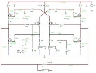
Ahhh ... yes, I see it ... the top MOSFETs (Q3 in your original schematic) are seeing identical signals, because they are connected to the same point under the CCS.
I inserted 100k resistors as per your suggestion (see attached schematic), so now Q3 sees a gate signal provided through C2. Bias for Q3 is provided through the 100k resistor.
Now the amplifier operates in 0/1 mode (using your terminology) with gain of about 4.
Is there a way to adjust to 1/1 or 2/3 mode (or in-between) without adding an extra transistor to segregate the differential drive to drive Q3? Adding another transistor is the obvious solution, but does the Zen Master see a hidden path?
(Also, the 100k resistors were added between the drain and gate.)
Attachments
Hmmm ... if a separate current source is used for each of the input devices (Q1 in your original schematic), then (a) the gate-to-source resistors wouldn't be needed?, and (2) the amplifier would act as two separate amplifiers, instead of a true differential amplifier.
Since my signal source is single-ended, a true differential input would be desirable, where the (-) input signal could be grounded and the (+) input could operate from a single-ended source.
The brute-force method would be differential pair input transistors, which adds another stage. I'd like to believe there's a more elegant solution ...
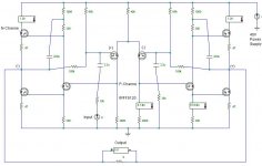
Yea, here's what happens when a single-ended signal is applied to the (+) input, as drawn on the schematic:
The input signal causes the (+) signal MOSFET to conduct a little more current. Both (+) and (-) signal MOSFETs (Q1) are powered with a common CCS. So when the (+) Q1 conducts more current, the current through the (-) Q1 decreases.
Back to the (+) side, the increased current through the 455 Ohm resistor creates a drive signal for the bottom (+) power MOSFET. This creates an inverted output signal. The top (+) power MOSFET responds to the output signal with an Aleph-like response through the 220uF feedback capacitor, which connects the top MOSFET's gate to the output signal. The top MOSFET is biased and DC-coupled through the 100k resistor.
Now at the (-) side, the decreased current through (-)Q1 also decreases the voltage drop across its 455 Ohm resistor, creating a differential drive to the bottom (-) power MOSFET. The output of the bottom (-) power MOSFET is fed to the top (-) power MOSFET through the 220uF capacitor. Again, the top (-) power MOSFET receives bias through the 100k resistor.
Therefore, the top power MOSFETs are always tracking the output signals through their AC coupling capacitors.
As explained, it all sees to work well and fine, but not what I'm looking for. It is permanently "stuck" in the 0/1 configuration as explained in the original PLH article.
Nelson Pass said:I have been presuming all along that your use of N channel
input devices was deliberate. Are you sure you weren't thinking
of P channel inputs?
The use of N-Channel was deliberate. I will work with understanding the value of using a P-Channel in this situation. At first glance, the only real change I see is some relationships are inverted, and no new relationships are created (however, a P-Channel device will give an inherent distortion canceling effect when combined with the N-Channel output devices). I will continue to pursue an "enlightened" solution to the problem of creating a truly differential amplifier without resorting to three stages. If three stages are used, one stage needs to be in source-follower configuration to avoid excess open-loop gain. A P-Channel could certainly be useful here, in the source-follower stage.
Fully balanced PLH schematic (link below), using 3 stages. The two signal stages are P-Channel. The output stage is N-Channel.
The center of the amplifier is a long-tailed phase splitter, with the 2000 Ohm resistors providing the bias voltage and AC signal for the second stage. (In this version, both are P-Channel).
I suppose this amplifier can be made using almost any combination of N-Channel and P-Channel signal transistors. To make the input stage a N-Channel, just flip the long-tailed phase splitter.
The IRFF110 (N-Channel) and IRFF9120 (P-Channel) are TO-39 transistors (they look like little water towers). Interestingly enough, the IRFF110 is one of the very few transistors produced by IRF that are specifically recommended for audio amplifiers.
The IRFF110 and IRFF9120 are also known as 2N6782 and 2N6845 from other manufacturers. I found some at Mouser.
Kashmire said:Yea, here's what happens when a single-ended signal is applied to the (+) input, as drawn on the schematic:
The input signal causes the (+) signal MOSFET to conduct a little more current. Both (+) and (-) signal MOSFETs (Q1) are powered with a common CCS. So when the (+) Q1 conducts more current, the current through the (-) Q1 decreases.
Back to the (+) side, the increased current through the 455 Ohm resistor creates a drive signal for the bottom (+) power MOSFET. This creates an inverted output signal. The top (+) power MOSFET responds to the output signal with an Aleph-like response through the 220uF feedback capacitor, which connects the top MOSFET's gate to the output signal. The top MOSFET is biased and DC-coupled through the 100k resistor.
Now at the (-) side, the decreased current through (-)Q1 also decreases the voltage drop across its 455 Ohm resistor, creating a differential drive to the bottom (-) power MOSFET. The output of the bottom (-) power MOSFET is fed to the top (-) power MOSFET through the 220uF capacitor. Again, the top (-) power MOSFET receives bias through the 100k resistor.
Therefore, the top power MOSFETs are always tracking the output signals through their AC coupling capacitors.
As explained, it all sees to work well and fine, but not what I'm looking for. It is permanently "stuck" in the 0/1 configuration as explained in the original PLH article.
Thanks for the explanation.
I'm still confused. To me, the gate-source of the (-) side upper
power mosfet looks bootstrapped against all ac voltages.
My misunderstanding . . . ?

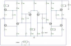
Schematic attached (I forgot to link it on Post #129). The circuit shown isn't fully tweaked, but may be close.
It is capable of +/-19 Volt (peak-peak) waveforms. I put bias at 1.25A at 40V for a total power dissipation of 100 Watts per channel. This puts 25W across each output device, so doubling up may be desirable. The bootstrap ratio on the second leg (1000:300 resistors) is somewhat arbitrary, but demonstrates flexibility.
The outputs are slightly biased downwards, so the (+) and (-) outputs rest at 15V. This leaves more headroom for the upper transistors work work in. Since this amplifiers is X'ed, it results in a symmetrical benefit that allows the +/-19V p-p output swing.
In the configuration shown, the closed-loop gain is about 10 V/V. DC coupled throughout.
Attachments
OK, so I'll go back and read about X'ing. I should write "...since this amplifier is balanced..." Need to work on my vocabulary.
Any comments on the actual schematic?
Regardless, the open-loop gain is too high and the feedback is too much. A lot of feedback is required to reduce the gain to 10V/V. The output impedance is too low. I found my speakers are sensitive to damping factor, and I think this design has too much DF.
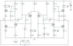
More specifically, the open-loop gain is about 200 V/V. This measurement is highly dependent on the series resistor at the input signal (open-loop schematic attached).
Any comments on the actual schematic?
Regardless, the open-loop gain is too high and the feedback is too much. A lot of feedback is required to reduce the gain to 10V/V. The output impedance is too low. I found my speakers are sensitive to damping factor, and I think this design has too much DF.
More specifically, the open-loop gain is about 200 V/V. This measurement is highly dependent on the series resistor at the input signal (open-loop schematic attached).
Attachments
Referring to Post #122
Correct ... both (+) and (-) upper power MOSFETs are AC coupled through the 220uF capacitors. In this mode, they function and constant current sources, and the signal is modulated by the bottom transistors. This is why it functions only in the "0/1 mode".
(Post #131 is adjustable, however. The 0/1 mode can be archived connecting the 220uF capacitor to the bottom of the 300 Ohms resistor ... aka the gate of the upper power MOSFETs.)
Babowana said:
Thanks for the explanation.
I'm still confused. To me, the gate-source of the (-) side upper
power mosfet looks bootstrapped against all ac voltages.
My misunderstanding . . . ?
Correct ... both (+) and (-) upper power MOSFETs are AC coupled through the 220uF capacitors. In this mode, they function and constant current sources, and the signal is modulated by the bottom transistors. This is why it functions only in the "0/1 mode".
(Post #131 is adjustable, however. The 0/1 mode can be archived connecting the 220uF capacitor to the bottom of the 300 Ohms resistor ... aka the gate of the upper power MOSFETs.)
Kashmire said:
Regardless, the open-loop gain is too high and the feedback is too much. A lot of feedback is required to reduce the gain to 10V/V. The output impedance is too low. I found my speakers are sensitive to damping factor, and I think this design has too much DF.
if you need a low damping factor from an amplifier isn't this indicating that your speakers are not optimum?
My present loudspeakers are just as finicky as any other pair I've built or bought. This includes Fostex single-drivers (which Pass uses with ultra-high output impedance current amplifiers) and my Linkwitz Phoenix system, which certainly has its own personality.
I should learn to keep my mouth shut and focus on the issue at hand. We should continue in the loudspeaker forum if we are to discuss this further.
Now, any word on the balanced PLH circuit? Did I use a P-Channel where an N-Channel would have been better? Any gross omissions? Is it possible to have a truly balanced PLH with only two stages?
Attachments
Trying to choose an amplifier based on damping factor is likely to lead to a great deal of frustration. One of the best amplifiers I ever owned for low end was a Conrad Johnson Premier One--a tube amp, hence fairly low in the damping factor sweepstakes--whereas some of the solid state pieces I've owned (with much higher damping factors) were lousy in the bass.
There's a lot more to it. For instance, the power supply must be robust if you want tight bass.
Don't blame the speakers, either way. There are numerous examples of excellent speakers with all sorts of Qs. Magneplanars and electrostatics are regarded by many as being difficult to drive, yet it's frequently just a case of getting the right amp.
(Yes, yes, yes...I know...the Magneplanars are purely resistive...I'm talking about the damping. Planar bass panels tend to be floppy if not controlled.)
Damping factor too high? That's an easy one. Stick a series resistor in line with the speaker. Or reduce the power supply. Or reduce the feedback. Or...
There are always options. It's just a case of making proper choices.
Grey
GRollins said:
There are always options. It's just a case of making proper choices.
Yes ... the path I was looking at was to reduce open-loop gain, therefore, be able to reduce the feedback ratio and still maintain a 10V/V amplification factor.
That being said, I'm quite interested if my overall schematic looks reasonable. Any comments?
Kashmire said:
Yes ... the path I was looking at was to reduce open-loop gain, therefore, be able to reduce the feedback ratio and still maintain a 10V/V amplification factor.
This is possibly a typical situation you are describing
 However, one of the reasons these simple, minimum number of stages, circuits work so well, is the inherant linearity of the circuit without F.B.
  Sometimes due to Linearizing techniques like source resisters, for instance, your problems compromise to resonable listening results. They improve the linearity but kill the gain. They have other benifits and disadvantages, but the gain goes down
 One other thing you may consider... A voltage gain of 3, is 10db, a gain of 10 is 20db, a gain of 30 is 30db, 100 - 40db, and so on, and you don't need anymore gain than 30db before you've built a couple 30db circuits... It will only get you in trouble or ??? Where were we... When did I use the phrase V/V?
That being said, I'm quite interested if my overall schematic looks reasonable. Any comments?
I'm going to give you a few minutes, probably more, but I don't want to mistakenly hurt feelings or start fruitless debates...
I'm no expert but I've learned a thing or two here and there...
Let's see... ... ...
First, I would want to see what FETs you had in mind??? There is no part #s???
Second(O.K. no counting) I remeber reading direct coupled, did I not? What are those 2.2'ufs???
What is that phase spliter? A P ch? I don't get it? It should be an N ch so the common souce voltage gain is driving the top side follower, and it also acts like a follower driving a common source bottom transistor. Will that p ch do that ???
O.K., without the middle stage being the way N.P. did it, or even JLH did it, It will likely slam to a rail
You will have positive feedback not negative according to your drawing (and/or my suggestion)... However, X'ing could work...How do you set and maintain a stable output and Iq?
I'm still staring at the 100k the 65k and the 5k...
It's a start
Kashmire said:Any gross omissions? Is it possible to have a truly balanced PLH with only two stages?
The feedback is positive, so think about switching the feedback
connections to the other output.
Yes you can have a truly balanced PLH with 2 stages. For
starters, you could simply build 2 PLH's and drive them balanced.
- Status
- This old topic is closed. If you want to reopen this topic, contact a moderator using the "Report Post" button.
- Home
- Amplifiers
- Pass Labs
- Plh