Hi, Baldin,
The PCB is here : http://www.diyaudio.com/forums/showthread.php?postid=1122850#post1122850
The schematic now is like ClassDfromRu's version 2.5
The PCB is here : http://www.diyaudio.com/forums/showthread.php?postid=1122850#post1122850
The schematic now is like ClassDfromRu's version 2.5
The coil in your filter will be radiating a lot of energy, as it is of an open type. I would try either a toroid or a closed ferrite core (RM or ETD or something).
But to check whether this is actually what is causing some of the problems, you could mount the one you have on a bit a way from the PCB (just very few cm's) and try turning it to see whether it has any positive or negative effect.
But to check whether this is actually what is causing some of the problems, you could mount the one you have on a bit a way from the PCB (just very few cm's) and try turning it to see whether it has any positive or negative effect.
Hi, Baldin,
I will try your advice. The inductor that I use is drum core, it radiates more than RM cores.
Is it toroidal cores radiates less than drum core? In RM cores the windings are contained/shielded between ferrites, but in drum core and ferrites the windings are open.
I will try your advice. The inductor that I use is drum core, it radiates more than RM cores.
Is it toroidal cores radiates less than drum core? In RM cores the windings are contained/shielded between ferrites, but in drum core and ferrites the windings are open.
lumanauw said:Hi, Zilog,
---- we want to make UCD, SMT component is a must, where we can have short tracks everywhere. Using ordinary components will lead to long tracks everywhere. -------
Before the mosfets blown, the sound becomes distorted first, and the current draw is rising very much. Why is this? Is there a shootthrough between top and bottom mosfets?
I completely dis agree on this..
")
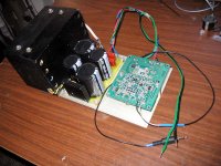
How come my UCD dont blow??
even at speaker loads of 2ohm and supply +/-45VDC @ 4A -and- with 100% through hole components..no need to torture...
just a test.... if it could do 2ohms....and IT DOES
until now its happily playing music with loads of 6ohms... I only have minimal heatsink.. still have NOT mounted in a suitable enclosure...
at present, Im just powering it up with +/-24V @4A.. to keep heat at minimum(even w/out fan)
I do have 30-0-30 @8A... but as of now , still have nowhere to play THOSE loud music if I power the diy with that 8A....
bigger transformer capacity = higher idle current(and thus HIGHER heat generated by FETs)..... bigger transformer(22A) = bigger heatsink = and a NICE BIG CASING === BIG BUCKS $$$$ = me (no more money for other projects)
power supply = 18-0-18 4A (+/-24V) with 10,000uF per rail...
the other module -resting- .....
both with OC and OV protection... I have DONE the DC protection circuitry(for speaker)and IS WORKING ALREADY.... but still not have made a board for it... Im currently busy with other electronics projects..
why do scopes have to be pricey...
cheers,
Raff
PS. send me the 22A transformer and I will happily test it....
just a test.... if it could do 2ohms....and IT DOES
until now its happily playing music with loads of 6ohms... I only have minimal heatsink.. still have NOT mounted in a suitable enclosure...
at present, Im just powering it up with +/-24V @4A.. to keep heat at minimum(even w/out fan)
I do have 30-0-30 @8A... but as of now , still have nowhere to play THOSE loud music
if I power the diy with that 8A....bigger transformer capacity = higher idle current(and thus HIGHER heat generated by FETs)..... bigger transformer(22A) = bigger heatsink = and a NICE BIG CASING === BIG BUCKS $$$$ = me (no more money for other projects)
An externally hosted image should be here but it was not working when we last tested it.
An externally hosted image should be here but it was not working when we last tested it.
power supply = 18-0-18 4A (+/-24V) with 10,000uF per rail...
the other module -resting- .....
both with OC and OV protection... I have DONE the DC protection circuitry(for speaker)and IS WORKING ALREADY.... but still not have made a board for it... Im currently busy with other electronics projects..
why do scopes have to be pricey...
cheers,
Raff
PS. send me the 22A transformer and I will happily test it....
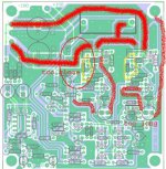
Hi, Fumac,
I try to analyze your suggestion. The marking "too long" = tracks for
- making 12V for (-Vrail+12V)
- tracks from differential to mosfet drivers
- rail tracks from capacitor bank to mosfets
- output of mosfets to inductor
"too close"
- the distance between rail tracks to mosfet driver section
Is my interpretation right?
What is the meaning of yellow circle you draw?
lumanauw said:Hi, Fumac,
I try to analyze your suggestion. The marking "too long" = tracks for
- making 12V for (-Vrail+12V)
- tracks from differential to mosfet drivers
- rail tracks from capacitor bank to mosfets
- output of mosfets to inductor
"too close"
- the distance between rail tracks to mosfet driver section
Is my interpretation right?
What is the meaning of yellow circle you draw?
the yellow circle is the g pin of fet, is Sensitive ,
too close to the Interference from the VDD and
the too long circle make ur Power of FET-driver is not very clean
this two reason make ur amp Self-shock in high power output
so the fet will burn
MY english not well to make u know me, soory for that , if u know chinese ,i will answer u in this link
http://groups.google.com/group/class-d-amp/
lumanauw,
make the mosfet driver/s CLOSER to the mosfet and make the GND planes much wider...
in short, make it more compact
less stray radiation....
sample/see below... its one of my earlier diy ucd... just the mosfet drivers/mosfets/filters.....
if you could make it THAT close, its much better...
make the mosfet driver/s CLOSER to the mosfet and make the GND planes much wider...
in short, make it more compact
less stray radiation....
sample/see below... its one of my earlier diy ucd... just the mosfet drivers/mosfets/filters.....
An externally hosted image should be here but it was not working when we last tested it.
if you could make it THAT close, its much better...
classd_fromru said:Hi all
RX5, its realy compact but totem pole not very closer (from fets to coil)
my testing kit
hi classd_fromru
i have told u that which type of fet that i used in my mcd
because the link was closed. i dont know if u know
rg
fumac
luka said:Hi
This is just crazy compact
I dont have access to SMD parts.. so I make the through hole components as close as possible..
but If ever something BLOWS, its a bit hard to desolder parts..classd_fromru said:Hi all
RX5, its realy compact but totem pole not very closer (from fets to coil)
my testing kit
IT does not really matter... I prefer the totem poles NEAR each other than either the COIL and mosfets... the COIL is just a filter...
underside of the above circuit... its still solderable...
my current PCB for my diy ucd STILL uses those tightly spaced layout...
and the UCD with the modulator board attached...(diff input)... still no protection and op-amp buffer BUT working...
now aint that small with through holes?
its still solderable... An externally hosted image should be here but it was not working when we last tested it.
my current PCB for my diy ucd STILL uses those tightly spaced layout...
and the UCD with the modulator board attached...(diff input)... still no protection and op-amp buffer BUT working...
An externally hosted image should be here but it was not working when we last tested it.
now aint that small with through holes?
Hi, Fumac,
I just experimented with my UCD-clone board. Before the worst mosfet is IRF540N. When I play the amp loud it only takes 1 second for the mosfet to blow.
I played with the gate resistors. Now I managed to make IRF540N not blown away with continious high level music, with Rg=220ohm. This is strange to me, the original Philips note uses only 22ohm for Rg. For IRF540N it has to be 220ohm, 10x the original value.
Fumac, is it OK to use 220ohm gate resistor?
But this comes with some expenses. First, the residual becomes 1V5 (p-p). Second, the gate drive (upper and lower mosfet Vgs) becomes triangle, not even close to square. But it survives for loud music now.
I guess IRF540N is not good for this cct. Using 220ohm Rg is actually slows down the turn-on. But in this case it is needed because the body diode of IRF540N is not good, slow (big trr), and have large Qrr. Using Rg=220ohm actually tries to minimize the cross-conduction, but sacrificing the dead time=worse THD.
The "chirping" bird sound is still there, I guess this is another problem with my board.
Fumac, what is the purpose of R24-C9, R23-C10 snubber? I change to 1nF+10ohm, it effects very little on the spikes on square edges.
Is there any other trick to remove the spikes on the square edges?
Hi, RX5,
Yes, it seems impossible, but it works. At first I also believe the value of Rg is 22ohm max. But there it is. Delay is only on the "on" side, while "off" is not affected (spaced by D11-D12 in UCD paper). 47ohm still cross-conduct. 100ohm still cross-conduct. 150ohm still cross-conduct. 220ohm, it stops.
Yes, it seems impossible, but it works. At first I also believe the value of Rg is 22ohm max. But there it is. Delay is only on the "on" side, while "off" is not affected (spaced by D11-D12 in UCD paper). 47ohm still cross-conduct. 100ohm still cross-conduct. 150ohm still cross-conduct. 220ohm, it stops.
- Status
- This old topic is closed. If you want to reopen this topic, contact a moderator using the "Report Post" button.
- Home
- Amplifiers
- Class D
- Philips UCD application note