Folks, I'd like an opinion please. The question is this:
When I lay out the silk screen, do people like to see the component value marked in the device body (this will be covered by the device when the board is stuffed, just intended as an aid during stuffing) and the designator placed so that it is visible when the board is stuffed, or is just the schematic designator only preferred?
When I lay out the silk screen, do people like to see the component value marked in the device body (this will be covered by the device when the board is stuffed, just intended as an aid during stuffing) and the designator placed so that it is visible when the board is stuffed, or is just the schematic designator only preferred?
Hi Jason,
I always place the comp ref des in silk somewhere on the comp perimeter, even when I make the footprint. Genrally, on the assy drawing layer, I place both value and ref des inside the comp body or the assy ref des to match where it is in silk layer.
For tight placement say 0805 or smaller it becomes a lot more work or impossible if it is too dense. Have to refer to the assy drawing or layout. The smallest silk text height I use is 50mil with a 5-6 mil line width.
Been doing this way for years without fail. You find these things out when you have to test your own creation and are pissed when you don't do it right correctly. It never hurts to add more information to the silk layer, to help guide you, when your memory fails you.
Rick
I also do a re-number of ref des in layout, top left to bot right and back annotate, can't believe what a treat it is to find the parts easily. Some cad pkgs are not so good at this task. Always do a project save, sometimes the back annotation and re-packager sw corrupts the database.
Its better to put reference next to component for when you might have to fix it later on.
I must admit I just put it in the middle of the component where it is hidden after component is mounted. However I usually use PCB software picture or a spare pcb for repairing.
Yes, I'm talking about the schematic reference being visible when the component is installed, but putting the value underneath as a stuffing aid.
Nigel, that is just cheating ") having a spare un-populated pcb in your hand.
having a spare un-populated pcb in your hand.
I remember doing some dense pcb's, we had to put a 21" monitor in the lab, so we could be able to tracing signals using cross-hilighting of comps/nets in the schematic, to where they were placed and routed on the mutli-layer pcb. This is a good as it gets.
Good feedback everyone.
having a spare un-populated pcb in your hand. I remember doing some dense pcb's, we had to put a 21" monitor in the lab, so we could be able to tracing signals using cross-hilighting of comps/nets in the schematic, to where they were placed and routed on the mutli-layer pcb. This is a good as it gets.
Good feedback everyone.
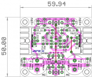
pretty old thread , but how abt this for a layout? I generally try to keep all traces as short as possible and thicker whenever required.
This layout already posted in APEX 100w ultimate amp thread, but re-posting here for convenience. Its an APEX design , servo pre-amp PSU.
any critic is welcome.
remember its a single side layout, I tried to optimize as much as possible.
JKT, some of your designs helped me learn.
regards
Prasi
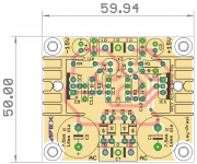
This layout already posted in APEX 100w ultimate amp thread, but re-posting here for convenience. Its an APEX design , servo pre-amp PSU.
any critic is welcome.
remember its a single side layout, I tried to optimize as much as possible.
JKT, some of your designs helped me learn.
regards
Prasi
Attachments
Last edited:
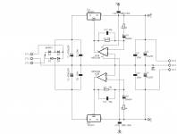
I could provide smd option on the bottom for C7, C8 like done for the op amp power pins.C7 & 8 are too far apart. The added trace lengths are increasing the impedance and as such prevent the decoupling do anything worthwhile.
I can identify the decoupling across the opamp power pins.
I agree with Suzyj and others. This is going to be a lot better with a ground plane on a second side. Current paths are shorter and have lower impedance. The low capacitance capacitors should always be placed as close as possible to the input/output of the regulator/amp IC.

- Home
- Amplifiers
- Solid State
- PCB Layout Process and Guidelines?