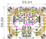
That leads me back to asking the same questions.I guess C9 and C10 are not doing anything useful at the positions where they are now.
Regards,
Oleg
What are the flow routes and return routes for the currents into C9 and C10?
Is that the correct question to help in analysing the opamp's HF decoupling effectiveness?
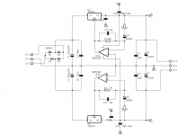
Had a good look through the forums and can't find the original description by apex of this psu topology. I assume that its a kind of output noise cancelling design?
here it is. http://www.diyaudio.com/forums/soli...imate-fidelity-amplifier-945.html#post5039079
there is no explanation.
This also shows the problem with the placing of C9 and C10.
does this help?
Attachments
i am wondering if my initial layout, with some mods in grounding (C7 to C10)would have been better! and it would have been diy friendly too!. + some mod to c1 c2 grounding, i would add, based on Jeff's recommendation...
let me work on it tomorrow evening, then i shall post the layout ...
let me work on it tomorrow evening, then i shall post the layout ...
Last edited:
There's always some compromise to a PC board layout. The design usually comes down to picking your priorities. In my designs I worry input connections to op amps, high current cap traces, decoupling cap connections to devices and grounding schemes as first priorities. Others will have other priorities, so they will see the layout as being wrong. In audio circuits I prefer to avoid ground planes due to the inability to control grounds. Sometimes it's nice to have a length of ground trace between a dirty supply ground and a signal ground. A plane doesn't allow you to do this.
It depends, are you concerned about the circuit oscillating or working as designed. Check the regulators and opamp datasheets for more info on the layout and stability.
Hi Mark,
Pl dont get me wrong. I am here to learn from pros and I was just wondering if that layout would have been better.
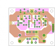
here is a version I made, but does the big ground surrounding the PCB components create a loop?
regards
Prasi
considerations,
1. does the ground follow current paths? yes, more or less
2. is decoupling clos to IC pins,? yes (added C16 and C13)
3. is the ground plane riddled with cuts, holes, discontinuieties?, no
Attachments
Last edited:
Look at the underside of the board JPS64 has designed. He has used maximum copper to reduce inductance.
https://www.saturnpcb.com/pcb_toolkit.htm is very helpful tool.
The inductance of a 1mm wide trace is about 12nH per cm length. If you increase the trace width to 10mm the inductance is reduced to 8.8nH/cm. Place a ground plane under the 10mm trace and you get 1.4nH/cm and that for free.
https://www.saturnpcb.com/pcb_toolkit.htm is very helpful tool.
The inductance of a 1mm wide trace is about 12nH per cm length. If you increase the trace width to 10mm the inductance is reduced to 8.8nH/cm. Place a ground plane under the 10mm trace and you get 1.4nH/cm and that for free.
Last edited:
I know its a little bit off topic but is no one inclined to comment on how this circuit actually works? Is it an Apex original design, or a generic circuit I haven't noticed before. You can buy pcbs from ebay if you're so inclined by the way. No idea if they're any good - waiting for my order to arrive.
I know its a little bit off topic but is no one inclined to comment on how this circuit actually works? Is it an Apex original design, or a generic circuit I haven't noticed before. You can buy pcbs from ebay if you're so inclined by the way. No idea if they're any good - waiting for my order to arrive.
Better to ask Mr. Mile in the thread where it originated.
Here its just serves as an example for layout.
Look at the underside of the board JPS64 has designed. He has used maximum copper to reduce inductance.
https://www.saturnpcb.com/pcb_toolkit.htm is very helpful tool.
The inductance of a 1mm wide trace is about 12nH per cm length. If you increase the trace width to 10mm the inductance is reduced to 8.8nH/cm. Place a ground plane under the 10mm trace and you get 1.4nH/cm and that for free.
Yes Mark , will do, thanks for your guidance.
Place a ground plane under the 10mm trace and you get 1.4nH/cm and that for free.
the final remark by Mark is referring to LOOP AREA.Yes Mark , will do, thanks for your guidance.
If you change the loop area you change the way emi is received/emitted.
Using that look at your latest layout.
If the ground trace is carrying return current at some instant in time, then what is the LOOP AREA for the Flow current + Return current?
An important condition for a plane to meet the "lowest impedance" requirement is that the Flow and Return currents must pass close to each other. Placing a gound plane on the top side of a two layer board inevitably results in a peppered plane that loses much of it's effectiveness because the Return current is forced to go find another higher impedance route.
A multilayer PCB using planes has 6thou to 10thou spacing of the planes. A 1.6mm thick two layer PCB has a spacing of >60thou. The loop area is already big.
Last edited:
An update,
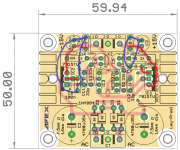
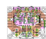
I got some time to revise, so here it is. the first pic shows only pads , bottom and top layer. the bright yellow trace......should it be connected or does it give rise to a loop around the edge of the pcb?
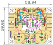
second shows the parts overlay.
There is some good info I found from a post by member marce , so posting link here.
Successful PCB grounding with mixed-signal chips - Part 1: Principles of current flow | EDN
I got some time to revise, so here it is. the first pic shows only pads , bottom and top layer. the bright yellow trace......should it be connected or does it give rise to a loop around the edge of the pcb?
second shows the parts overlay.
There is some good info I found from a post by member marce , so posting link here.
Successful PCB grounding with mixed-signal chips - Part 1: Principles of current flow | EDN
Attachments
Last edited:
- Home
- Amplifiers
- Solid State
- PCB Layout Process and Guidelines?