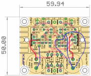
If both C7 and C8 are rotated 180degrees, then there may be a path between the two.
There is a path from the label IC2 to the label C5
Get C7 ground pin on to the other side of the traces so that it is beside the C5 label.
There is a path from the label IC2 to the label C5
Get C7 ground pin on to the other side of the traces so that it is beside the C5 label.
The trace from D2 to D1 could run under the diodes instead of parallel to the trace going to IC3.
Any opinions on moving C9/C10 near to the IC? Looks wrong to me.
Any opinions on moving C9/C10 near to the IC? Looks wrong to me.
Are C9 & 10 attached to the ground plane via the through hole pinning of Pins 3 & 5?
I think the decoupling should have their own connections to the ground plane.
I think the decoupling should have their own connections to the ground plane.
If you rotate C7 180 degrees it will be better still.
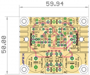
Ok, so finally here is a killer layout 😀. Only 4mm distance from 0.1uF cap to regulator pin. using a smd would make it better still.
To Andrew,
there is no option but to lay a trace from capacitor to 7815 in. personally I do not like 2 sided boards and ground planes, but if it helps to make a perfect 5$ chinese PCBs, I am game.
like my F5 headamp layout, although 2 sided, i didnt use a gnd plane as advised by someone. it works perfect, absolute silence as reported by builders (2 that I know of).
regards
Prasi
Attachments
The trace from D2 to D1 could run under the diodes instead of parallel to the trace going to IC3.
Any opinions on moving C9/C10 near to the IC? Looks wrong to me.
Hi Mark,
Would it matter much? all the charge is stored in the caps and they supply the regs and its 24V at that place. The clearances are are about 0.762 mm. I think it should be sufficient...
reg
Prasi
Last edited:
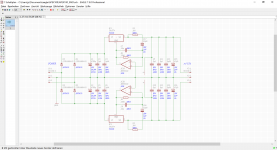
Ground planes can be tricky to use. If they are under feedback components on some op amps they can actually cause oscillation. Some data sheets will mention this. It might be safer to make the area under R2, R3, C11 and C12 a keep out zone.
Hi Mark,
Would it matter much? all the charge is stored in the caps and they supply the regs and its 24V at that place. The clearances are about 0.762 mm. I think it should be sufficient...
reg
Prasi
The current through the diodes to the capacitors consists of 100 short spikes per second with an amplitude 8 to 10 times higher than the DC current from the capacitors to the load. Very important to keep these traces away from others. Also, remember that these currents flow in the return path too.
Starting with schematics, using software with real time backannotation, like Eagle. Big library is helpful. Undo/Redo, and good editing functionalities also. You need a good knowledge about existing and available market components (searching Farnell, Mouser, Digi-Key, others: personally I´m using the Firefox plugin Ciiva).
In this example, I´m mixing SMD and THT then board dimensions are small and the heatsinks needs space. Some components fixed THT such as the big 4700µF/35V capacitors or regulators with heatsinks).
I don´t care about placement side, board is 2 layer (no extra charge today) and I´m intending to use massively copper areas and top/bottom SMD placement.
Placement and routing configuration mil, mm, inches as you want. Years ago, placing was exclusively done in inches, today, newest components are in mm. DIY don´t care about this, the board will never go in series. I´m placing in millimeters and doing optimisation down to 0.05mm (also for series and component placement datas for manufacturers). Starting with 1mm, routing with 0.5mm and finish the job if necessary with 0.05mm.
PCB manufacturer offering standardly and for good price 0.2mm clearance and minimal via drilling.2 layer 35µm copper, green solder resist, white silkscreen are standard. Via filling is available at extra charge. Multi-cb supplies short but clear PCB rules.
Rough component placement is following. I´m spending generally a lot of time for the placement and don´t hesitate to replace SMD parts by THT parts and inversely. A good placement is 90% of the job.
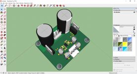
Quick 3D check with sketchUP.
First steps, more to come if wanted?
P.S.: going back to my 833C amplifier layout routing.
P.P.S.: @prasi What heatsinks are you using?
P.P.P.S.: for clearance... https://www.mikrocontroller.net/articles/Leiterbahnabstände
JP
In this example, I´m mixing SMD and THT then board dimensions are small and the heatsinks needs space. Some components fixed THT such as the big 4700µF/35V capacitors or regulators with heatsinks).
I don´t care about placement side, board is 2 layer (no extra charge today) and I´m intending to use massively copper areas and top/bottom SMD placement.
Placement and routing configuration mil, mm, inches as you want. Years ago, placing was exclusively done in inches, today, newest components are in mm. DIY don´t care about this, the board will never go in series. I´m placing in millimeters and doing optimisation down to 0.05mm (also for series and component placement datas for manufacturers). Starting with 1mm, routing with 0.5mm and finish the job if necessary with 0.05mm.
PCB manufacturer offering standardly and for good price 0.2mm clearance and minimal via drilling.2 layer 35µm copper, green solder resist, white silkscreen are standard. Via filling is available at extra charge. Multi-cb supplies short but clear PCB rules.
Rough component placement is following. I´m spending generally a lot of time for the placement and don´t hesitate to replace SMD parts by THT parts and inversely. A good placement is 90% of the job.
Quick 3D check with sketchUP.
First steps, more to come if wanted?
P.S.: going back to my 833C amplifier layout routing.
P.P.S.: @prasi What heatsinks are you using?
P.P.P.S.: for clearance... https://www.mikrocontroller.net/articles/Leiterbahnabstände
JP
Attachments
JP,
nicely done. I stick to 0.254mm grid if not 0.508mm grid. Makes routing easy.
The heatsinks are available in all electronics shops here and also in aliexpress
https://de.aliexpress.com/item/10pc...32454598520.html?spm=2114.47010208.4.2.WvLX4r
nicely done. I stick to 0.254mm grid if not 0.508mm grid. Makes routing easy.
The heatsinks are available in all electronics shops here and also in aliexpress
https://de.aliexpress.com/item/10pc...32454598520.html?spm=2114.47010208.4.2.WvLX4r
I'm inclined to agree with you that ground planes don't have much benefit (if any) for audio frequency circuits.Ok, so finally here is a killer layout 😀. Only 4mm distance from 0.1uF cap to regulator pin. using a smd would make it better still.
To Andrew,
there is no option but to lay a trace from capacitor to 7815 in. personally I do not like 2 sided boards and ground planes, but if it helps to make a perfect 5$ chinese PCBs, I am game.
like my F5 headamp layout, although 2 sided, i didnt use a gnd plane as advised by someone. it works perfect, absolute silence as reported by builders (2 that I know of).
regards
Prasi
But there are some current changes that are way above audio frequencies.
Just how high must these frequencies become before a plane starts to offer benefits?
Now back to your layout.
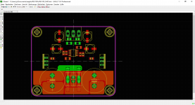
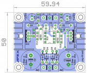
I can't see the link from C7 ground pin (1) to C8 ground pin (2). Can you add that so that we can see how long/short it is?
Last edited:
I'm inclined to agree with you that ground planes don't have much benefit (if any) for audio frequency circuits.
But there are some current changes that are way above audio frequencies.
Just how high must these frequencies become before a plane starts to offer benefits?
Now back to your layout.
I can't see the link from C7 ground pin (1) to C8 ground pin (2). Can you add that so that we can see how long/short it is?
The whole bottom layer is ground plane.
The "whole" bottom layer is riddled with cuts, slots and linked holes.The whole bottom layer is ground plane.
Where is the low impedance return current route that follows the flow current?
Where is any return current route, even if it does not follow the flow current?
I cannot see it because the holes and cuts are disguised under the components.
There's only one short trace on the bottom layer. There are holes but still mostly complete copper plane.
Can you trace out the route and show me what you can see?There's only one short trace on the bottom layer. There are holes but still mostly complete copper plane.
Can you trace out the route and show me what you can see?
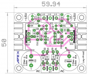
Here is the image of top and bottom layer . I have it slightly modified based on your , Jeff and Mark's advice.
Attachments
Can you trace out the route and show me what you can see?
Two loops. Blue is the ground plane return path.
Attachments
Last edited:
Two loops. Blue is the ground plane return path.
Mark, does my layout in post 136 takes care of that?
Or does the restrict area around the op amp makes a loop?
Now I can clearly see a route from C7 to C8. The HF power ground is somewhere near the label "X2"
Repeat for the Flow currents into C7 and C8. Do the Flow currents and Return currents pass along traces/routes that stay close to each other?
Next. Repeat the tracing process for the MF decoupling (in this case the same as the PSU smoothing since it is on board).
The MF decoupling power ground and the PSU power Ground are somewhere around the area under the power diodes.
Note that the MF decoupling ground and the HF decoupling ground are massively separated. What would be the voltage difference between those two grounding areas?
It cannot be zero. Using a plane has NOT helped in keeping the grounds at similar voltages.
The purpose of a ground plane is to minimise the impedance between connections. Here we see something different.
Maybe I am asking the wrong questions.
Maybe what I expect to see by implementing a ground plane is impossible to achieve. Because I don't know enough.
I know that I don't know enough about implementing ground and power planes that I don't attempt to design them into any circuit I do. I use direct wire, or trace, connections where I can control the routes and the locations of virtual reference points.
Last edited:
- Home
- Amplifiers
- Solid State
- PCB Layout Process and Guidelines?