andy_c said:If you need a SPICE model for the BAV21, it is here.
Thanks Andy,
I'm trying to understand why the model for the BAV21 I have doesn't give the expected results, but the model for the MUR115 does. I am trying to work up a new component with your model, but it's not happening yet. For some reason, when I get the new component finished and saved, the model is not attached.
I'll figure it out. Just something else to irritate me.


Capacitive load test came up aces.
I connected a 1.2uF cap for the load only (no resistance). No change - still runs completely stable. Clipping is not as nice, but nothing overly bad.
Upped it to a 2.4uF cap. Still no change in stability. Clipping has the bottom wave part colapsing, and a big jump in current draw, so I'll avoid doing that again. Leach advises a stable amp should be able to drive a 2uF cap:
The original version of this amp had some severe ringing when driving a much lower cap.
Not bad, I guess.
All this without the Thiele or Zobel networks.
Getting closer to the "Nirvana" that Nico talked about.")
I connected a 1.2uF cap for the load only (no resistance). No change - still runs completely stable. Clipping is not as nice, but nothing overly bad.
Upped it to a 2.4uF cap. Still no change in stability. Clipping has the bottom wave part colapsing, and a big jump in current draw, so I'll avoid doing that again. Leach advises a stable amp should be able to drive a 2uF cap:
-W. Marshall LeachA good indicator of an amplifier sound quality is its ability to drive a capacitive load. The classic example of a capacitive loudspeaker transducer is the electrostatic transducer. Another is the piezoelectric transducer used in some horn tweeters. I have heard of amplifiers overheating when driving arrays of these tweeters. No doubt the circuits were oscillating. A third source of load capacitance that is often overlooked is the loudspeaker cable. Some of the so-called "high definition" cables are designed to minimize the series inductance. Because the series inductance per unit length multiplied by the shunt capacitance per unit length is a constant that is equal to the reciprocal of the velocity of light squared, minimizing the inductance maximizes the capacitance. Therefore, these cables can exhibit a high shunt capacitance. For this reason, I generally do not recommend them.
The Low TIM amplifier is stable with capacitive loads. I have tested it with a 2 uF capacitor. This is a test that I learned from reading Bascom King's reports on amplifiers for Audio (rip) magazine back in the '70s, and it is probably the worst load that I know of. Because some amplifiers become unstable with a capacitor for a load, I have seen the test made with a resistor, e.g. a 2 ohm resistor, in series with the capacitor. This is cheating. It does not indicate the stability of the amplifier to a capacitive load. The first time I tested my prototype Low TIM amplifier with a 2 uF capacitor, it blew the 0.33 ohm 5 W emitter degeneration resistors in series with the output transistors. I suspect the circuit was oscillating. Either the resistors couldn't handle the current or the circuit was oscillating. I suspect the latter.
Another good indicator of an amplifier sound quality is its high frequency clipping behavior. When an amplifier is driven into clipping, some of the transistors in the circuit are driven into saturation. When a transistor saturates, a relatively large charge is stored in the semiconductor junctions. For the amplifier to come out of clipping, this charge must be neutralized. To minimize the time for this to occur, the larger output and driver transistors should never be allowed to saturate. Although the power rating of an amplifier can usually be increased if the output transistors are allowed to saturate, it causes a high frequency clipping problem that has been described as "sticking." When an amplifier exhibits this problem, its output waveform appears to become "stuck" at the clipping level when it is driven into clipping at high frequencies. In the Low TIM amplifier, the transistors which saturate are in the second stage of the amplifier. As a result, the circuit does not exhibit high frequency sticking problems when it is driven into clipping.
The original version of this amp had some severe ringing when driving a much lower cap.
Not bad, I guess.
All this without the Thiele or Zobel networks.
Getting closer to the "Nirvana" that Nico talked about.
homemodder said:Looking good indeed, can you post schematic with all the chaanges you made so far.
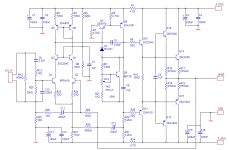
Here it is.
Fresh new look.
Attachments
MJL21193 said:
Hi Andrew,
It's not sticking though - it's recovering immediately. The VAS is not saturating, just the EF.
John, I would say that it is "sticking". Note the length of the pos flat top, versus the neg flat top. If you overlay a perfect sinewave on your clipped waveform I'd expect the pos clipping to extend ("stuck") past the point where the sinewave heads back to zero. The front end overloads around that point because the output is not following the input, and when the VAS finally recovers, that high slope edge is where it "catches up" to where it should be. This sticking is also referred to as charge storage, and the feedback loop time constant changes when the VAS saturates which probably explains the ringing as it comes out of clipping. I've looked at this in some detail as I think we discussed in your original thread where I suggested a Baker clamp.
It can help in understanding to take a look around the diff pair and EF to see how the VAS is driven while in overload.
Pete B.
mlloyd1 said:john:
it's fun looking over your shoulder.
thanks for sharing!
Thanks mlloyd1,
It goes both ways - I get a cheap "education" and have fun myself doing it.
PB2 said:
John, I would say that it is "sticking".
It can help in understanding to take a look around the diff pair and EF to see how the VAS is driven while in overload.
Hi Pete,
I was off in the terminology again. I thought that "sticking" was where it would hit the rail and stay there. My mistake.
In the simulation, it looks as though the EF is saturating. The VAS looks normal. I didn't look at the differential pair to see what is going on there - I just assumed that it was functioning normally. Do you think that there is some way to minimize this clipping behavior, before the Baker clamp?
In the original thread, I couldn't get the Baker clamp to work in the simulation, remember? I managed to get it working in this simulation by trying different diodes (models). I'm baffled by this. Andy's model for the BAV21 will not work properly in my sim, neither will the Multisim version. I've had luck with the MUR115.
Long and short is that the clamp works fine in the actual amp. It doesn't effect the stability and doesn't seem to have an adverse effect on sound quality. In the simulation, distortion increases slightly, but I have room to spare in this regard.
MJL21193 said:Do you think that there is some way to minimize this clipping behavior, before the Baker clamp?
In the simulation I probed the base of the EF. When at near full unclipped output, I have ~450uA. With mild clipping nearly 2mA.
By increasing the emitter degeneration resistors in the diff pair I can minimize this current jump. I took the value from 33R to 200R.
Am I on the right track here?
MJL21193 said:In the simulation I probed the base of the EF. When at near full unclipped output, I have ~450uA. With mild clipping nearly 2mA.
By increasing the emitter degeneration resistors in the diff pair I can minimize this current jump. I took the value from 33R to 200R.
Am I on the right track here?
Hi John,
The emitter resistor change will make the GBW lower by a factor close to 33/200 and will increase the distortion by roughly 200/33., so it's not the right thing to do.
This also raises the question of why there is a collector resistor in the EF. Was that for power dissipation reasons? With no collector resistor, it can't saturate. Saturation for a PNP happens when the collector voltage is higher than the base. That's how the Baker clamp fixes the problem for the VAS CE stage. It clamps the collector voltage so that in the worst case, the collector is at a voltage the same as the base. When the collector-base junction becomes forward biased (P positive with respect to N), that's what causes the big increase in base current. Think of it as an internal diode between collector and base, with the cathode connected to the base and anode to collector. When this diode becomes forward biased, a big increase in base current occurs.
For the BAV21 diode model, try removing the NBV parameter. That's a PSPICE-specific extension also supported by LTspice but maybe not your simulator.
andy_c said:
Hi John,
The emitter resistor change will make the GBW lower by a factor close to 33/200 and will increase the distortion by roughly 200/33., so it's not the right thing to do.
Yes, this is how it plays in the sim - increased distortion. I don't want to do this, just trying to understand what's happening. The current jumps because the EF is saturating, and is not the cause of the saturation, right?
andy_c said:
This also raises the question of why there is a collector resistor in the EF. Was that for power dissipation reasons?
Yes. The resistor goes back to the original thread, where we discussed the ways and means to protect the VAS. Pete (PB2) suggested the collector resistor to limit current in the EF.
In the sim, when I take out that resistor, the VAS goes into saturation instead, and the current draw is much higher.
Also, when I eliminate this resistor in the sim, the Baker clamp diode no longer works. I tried a few different things in the actual amp yesterday, like reducing the emitter resistor (R5) but found I ran into stability problems. This may be due to the way I did these changes - tacking a long leaded resistor in parallel with the existing but I doubt it.
I will try the actual amp with R7 shorted and see how it goes.
MJL21193 said:I will try the actual amp with R7 shorted and see how it goes.
I tried that and it made no difference. Same clipping (without the clamp) with or without this resistor.
Maybe I should accept what I have. The clamp nicely takes care of the clipping issue; the amp runs ultra stable, even into a capacitive load; simulated distortion is ultra low; reliability seems to be high and sound quality seems to be quite high.
After, why fix it if it's not broken?
I just completed the first full power trial on this new board. The Baker clamp is just "friction fit" between the leads of the Miller cap and the drivers are not bolted to the heatsink so I don't want to push it. I'll take it off the heatsink later and solder the clamp in semi-permanent place (until I get the BAV21's).
The metal tab on the TO-220 is really inconvenient - requiring a plastic shoulder washer to insulate. I like the plastic of the TO-264 and TO-126 much better. No worries about wearing trough the thin plastic of a shoulder washer while installing the screw.
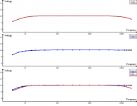
Getting back to the bootstrap topic: I did an interesting test this morning. I needed to put a face on the supposed limitations of this topology. Possibly, all of this has been done before, with much more methodical and exhaustive testing done.
I thought I would measure the voltage at the junction between the top bootstrap resistor, the base stopper to the Q11 driver and the Vbe multiplier. I thought I could just measure the AC voltage here and sweep the frequency up from low to high, taking note of the values. I set the output of my function generator to a sine wave at 20Hz and adjusted the amplitude to give me 10VAC at that junction. I called this my baseline.
From here I dropped to 18Hz and took note of the voltage. Then to 16Hz and so on down to 4Hz, taking measurements as I went.
I then swept upwards to 20kHz, taking measurements all along the way.
To my way of thinking, this effectively maps the linearity of the bootstrap over the swept frequency range.
I then did the exact same test with the simulation of this amp, using my RLC mockup in place of the bootstrap cap.
The results are below. Top is the charted voltage at frequency of the top bootstrap resistor.
The middle is the same in the simulation and the bottom is one over the other for comparison.
Thoughts?
Attachments
MJL21193 said:
In the simulation I probed the base of the EF. When at near full unclipped output, I have ~450uA. With mild clipping nearly 2mA.
By increasing the emitter degeneration resistors in the diff pair I can minimize this current jump. I took the value from 33R to 200R.
Am I on the right track here?
Let me just point out that you seem to be looking for a solution to the current jump as if it is a problem. It would probably help to step back and think about this - you have a high gain amp where the gain is used to correct for distortion/errors in the output - if the output ever cannot track the input with low distortion then the high gain amp attepts to produce a large correction voltage/current. The output cannot follow the input in clipping, slewing, and when it is shorted and therefore the front end tries to produce a large (overload) correction.
I believe that it is an oversight not to include R7 as from what I saw the EF and VAS can fail without a protection transistor. I would probably leave in R7 even with an EF/VAS protection transistor. Its important to also look at what the amp does with a shorted output as we discussed in the original thread.
You ask about the LTP degeneration resistors - you're lowering the gain when you increase their value and making the front end more linear in overload. However, as Andy pointed out lowering the gain increases distortion. Its a tradeoff.
If the amp has high enough slew rate, current limiting during clipping and for a shorted output, and recovers cleanly from overload then it seems that there is no reason to increase the LTP emitter degeneration resistors beyond the value that provides the lowest distortion. They do also make the design less sensitive to diff pair mismatch which is not an issue if you match devices.
It is looking good John, like a JE-990 converted to a power amp, with some nice improvements. Cascoded LTP, jcx's trick of bootstraping the LTP, and R7 to improve overload handling/recovery. I remember that you removed the bootstrap to the cascode reference based on simulation results, but I have to wonder if this agrees with real hardware - a minor point.
Pete B.
I don't think I can take credit for bootstrapped tail current souces, they predate my birth date
If I were modding what I see in the last schematic I would go for more current gain by using cfp driver stage and high enough bias that it would always be in solid Class A
this should increase gain by presenting higher impedance VAS load, the VAS bootstrap would give a higher Z if the C were moved to the lower driver emitter
the tail bootstrap R ratio needs to be readjusted to give the new higher current and have the correct divider ratio == feedback divider ratio
and while not "simple" I would play with TMC or 2-pole compensation to put more of the (increased) loop gain in the global loop at audio frequencies where it improves both input and output stage distortions
PB2 said:
I believe that it is an oversight not to include R7 as from what I saw the EF and VAS can fail without a protection transistor. I would probably leave in R7 even with an EF/VAS protection transistor. Its important to also look at what the amp does with a shorted output as we discussed in the original thread.
It is looking good John, like a JE-990 converted to a power amp, with some nice improvements. Cascoded LTP, jcx's trick of bootstraping the LTP, and R7 to improve overload handling/recovery. I remember that you removed the bootstrap to the cascode reference based on simulation results, but I have to wonder if this agrees with real hardware - a minor point.
Hi Pete,
R7 stays. Clipping performance is not improved by it's removal. I like how it limits the current through the EF, and by extension, the VAS.
Thanks. Everytime I do a new or improve amp project I pick up a few more things. Still, a long way off in my understanding and it shows I expect.
What drive me onward are tangible results - I need that working unit in front of me. I also, if I don't mind saying so, have a talent (it must be talent, as I don't actually know enough) for sniffing out the cause of problems.
For example: It turns out that this latest board, with all of the tests that were done, had a blown ballast resistor. R17 on Q14 was open. I discovered this when I tried to set up the idle current. The voltage across this one read 408mV, while the one next to it had 15mV. It didn't occur to me that the emitter resistor could be open, and I was getting ready to pull the output, thinking it was faulty. What made me measure the resistance of the resistor? I don't know.
I have more faith in the simulator now than I did before, especially where the distortion measurements are concerned. The feed-forward to the cascode would always increase distortion, no matter how I configured it. This was even more apparent when I learned how to use the Fourier analysis, giving much higher resolution.
In contrast, the bootstrap to the LTP would lower distortion. It was just a matter of hitting on the correct value for the resistor.
Now, the amounts involved are relatively small, but it's all cumulative and it makes up for the small amount of distortion introduced by the Baker clamp (this may or may not be accurate, given my troubles with diodes in this simulator).
jcx said:
the VAS bootstrap would give a higher Z if the C were moved to the lower driver emitter
Now you tell me! I guess this is something that i should have known.
It makes sense - even though I have selected fast outputs, there would still be a lag between driver and output.
I will see about implementing this.
jcx said:
If I were modding what I see in the last schematic I would go for more current gain by using cfp driver stage and high enough bias that it would always be in solid Class A
this should increase gain by presenting higher impedance VAS load, the VAS bootstrap would give a higher Z if the C were moved to the lower driver emitter
the tail bootstrap R ratio needs to be readjusted to give the new higher current and have the correct divider ratio == feedback divider ratio
and while not "simple" I would play with TMC or 2-pole compensation to put more of the (increased) loop gain in the global loop at audio frequencies where it improves both input and output stage distortions
Let me understand what it is you are saying: The drivers themselves, not the outputs, in class A operation?? I like it!
BUT,
Lets save some of those for the sequel! There's V4 to think of...
If you have trouble with sticking on the bootstrap side you can add a diode to clamp the voltage so it can only go outside the rail by 1 diode drop. Then you put one diode in series with the feed from bootstrap circuit to VAS so that the voltage on the driver base/bias spreader is clamped at rail voltage. This prevents saturation in the driver transistor.
andy_c said:
Hi John,
The emitter resistor change will make the GBW lower by a factor close to 33/200 and will increase the distortion by roughly 200/33., so it's not the right thing to do.
Though if you reduced the miller compensation capacitor to bring the unity loop gain frequency back out to where is was the distortion should be relatively unchanged above the dominant pole. In fact it might be slightly less at HF due to the reduced loading on the VAS.
Cheers,
Glen
G.Kleinschmidt said:Though if you reduced the miller compensation capacitor to bring the unity loop gain frequency back out to where is was the distortion should be relatively unchanged above the dominant pole. In fact it might be slightly less at HF due to the reduced loading on the VAS.
Hi Glen,
Here's some experiments I've done in the simulator and what I've found. This used a configuration like the "Blameless" amp.
1) Configuration 1: Input and output stages modeled as ideal controlled sources, and VAS the same as the real design. Vary input stage gm and VAS Cdom simultaneously so as to keep the GBW constant. Look at full power 20 kHz THD.
2) Configuration 2: VAS and output stages modeled as ideal controlled sources, with input stage the same as the real design. The idealized VAS input impedance, transconductance and input DC offset from the rail were made the same as the actual VAS. Vary input stage gm and VAS Cdom simultaneously so as to keep the GBW constant. Look at full power 20 kHz THD.
For configuration 1, using reasonable values of Cdom (< 200 pF), the larger Cdom was made, the lower the distortion was. I assume that the increase in the loop gain of the Miller loop due to increasing Cdom was responsible - apparently winning out over the increased VAS loading.
For configuration 2, the larger Cdom was made, the larger the distortion was. Clearly this was the result of the capacitive loading of Cdom on the input stage. Input stage distortion was very low, but this wasn't achieved until I used bootstrapped cascoding of the input stage.
Now suppose the whole amp were simulated, starting with larger than usual input stage emitter degeneration and small Cdom. Suppose you simultaneously decrease emitter degeneration and increase Cdom to keep GBW constant. My guess was that the 20 kHz full power THD would keep decreasing up to the point where input stage distortion started to overtake VAS distortion. Then, as further decreases in input stage emitter degeneration were made, the distortion would begin to increase again. This is exactly what happened. I stepped Cdom over a list of standard capacitor values, recomputing input stage RE at each step. There was a combination of Cdom and input stage RE that gave the best 20 kHz THD. For larger or smaller Cdom (with RE adjusted appropriately), the full power 20 kHz THD increased. So I ended up using the Cdom and RE that were optimized in this way. For this specific design, Cdom was 68 pF - nothing at all radical.
- Status
- This old topic is closed. If you want to reopen this topic, contact a moderator using the "Report Post" button.
- Home
- Amplifiers
- Solid State
- Patchwork Reloaded: Circuit Optimization and Board Layout.