Member
Joined 2009
Paid Member
ESP P3a specifies a TO92 too. It doesn't even contact the drivers or their heatsink but works with an appropriate tempco quite reliably, if you take care to locate it nearby. I did mount mine in thermal contact, as Sakis showed with his board in the first P3a thread but that's long been proven unnecessary...... Strange choice for Q9 (Vbe), it's a high voltage TO-92 part. You'd be better off with a TO-126 part for bolting to a driver device for thermal management. And ideally the Vbe device would be a high-beta device that's happy to operate with a low voltage across it. What's wrong with the BD139/140 family ?
Still, I'm uncertain about the best tempco being maintained in either case and distance does slow response time and admits radiation from the output transistor heatsink to complicate matters. The slow warm-up time for bias settling can't be a good thing either.
when the source impedance is low then one generally obtains lower output noise when the tail current is increased.
that's the ooposte to what AJT just posted.
We generally connect lowish source impedances to out power amp inputs. So it follows that higher tail current equals lower noise.
that's the ooposte to what AJT just posted.
We generally connect lowish source impedances to out power amp inputs. So it follows that higher tail current equals lower noise.
Did none of you bother to read
Q5+Q6+Q9 should be on a common heatsink/plate.
Did none of you bother to read
The original design recommends to position Q9 near one of the drivers and not on the outputs heatsink.
Cheers,
Jacques
The original design recommends to position Q9 near one of the drivers and not on the outputs heatsink.
Cheers,
Jacques
you need to do a bit more reading understanding the principal of operation of the P3A might look simple but actually is not that simple after all
Most of people see the schematic and think EFP wise ... that is the first mistake
Most of people see the schematic and think EFP wise ... that is the first mistake
Very true: P3A boasts Sziklai pair aka CFP.
Could also try a collector load on Q2 to balance Vc at both ltp devices - neve tried it myslf but SandyK of years past said it kept the Early Effect matched when he was tweaking the AKSA amplifier.
I did try it in simulation but it does not show much effect in current balance, I think Rod does not recommend putting a resistor there.
Did none of you bother to read
Yes, this is exactly what I did in my actual build, just applied a small amount of thermal grease on the TO-92 VBE multiplier.
using a matched pair and then operating them at different power dissipations is a waste of resources.I did try it in simulation but it does not show much effect in current balance, I think Rod does not recommend putting a resistor there.
The idea of a matched pair is to have identical Ic, Ie Ib, Vbe, Vce and Vcb
When these are all identical you have the same dissipation in each half and when Thermally coupled they operate at the same temperature.
Maintaining the same temperarture, both Tj and Tc is what allows the LTP amplifier to achieve low distortion and accurate feedback correction. The feedback effectively subtracts from the input to give that desirable Zero differential voltage between +IN and -IN.
If you omit the collector resistor on one side of the LTP, then that side has a higher Vce and thus no longer has equality of temperature between the two junctions. You have unmatched your matched pair.
Thanks Andrew,
Thats a lot of help.
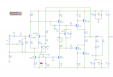
I am departing from my originally planned P3A mod. I thought it was pretty inconvenient and misleading from the original design. I am going to attempt to design one CFP, I know this is going to be hard. I am showing the schematic I have drafted, it looks pretty generic and it could also mean a complete failure but it shows some good results in simulation.
Sorry Sakis I am going to be out of topic, for the moment.
Thats a lot of help.
I am departing from my originally planned P3A mod. I thought it was pretty inconvenient and misleading from the original design. I am going to attempt to design one CFP, I know this is going to be hard. I am showing the schematic I have drafted, it looks pretty generic and it could also mean a complete failure but it shows some good results in simulation.
Sorry Sakis I am going to be out of topic, for the moment.
Attachments
I never thought about noise before, at least the issue with higher tail current instead seems to me to be related to having use a smaller collector load which reduces OLG.
Could also try a collector load on Q2 to balance Vc at both ltp devices - neve tried it myslf but SandyK of years past said it kept the Early Effect matched when he was tweaking the AKSA amplifier.
Leach mentions it in his double barreled amp article in Audio magazine in 1980...
Leach used 4mA tail currents, AKSA otoh prefers much lower tail currents...
Change R8 to two 8k2 in series.
Connect the junction of these two resistors to -Ve supply rail using a 100uF 50V electro.
Q10 is running @ ~250mW, why use a medium power transistor?
Either use a 5551 @ 4mA, or use the bd at 8mA to 10mA
Adding Q10 has moved this from a P3A
Give it it's own Thread.
Connect the junction of these two resistors to -Ve supply rail using a 100uF 50V electro.
Q10 is running @ ~250mW, why use a medium power transistor?
Either use a 5551 @ 4mA, or use the bd at 8mA to 10mA
Adding Q10 has moved this from a P3A
Give it it's own Thread.
Last edited:
Yes, you have increased the open loop gain and increased the feedback.Hi, I just run an LTSpice simulation and making R20 to be 10R, bypassed by 1 to 10uF, has a positive effect on THD
You have seriously reduced the stability margins and the amplifier may oscillate, or at the least, sound brittle due to excessive overshoot on fast changing signals.
Member
Joined 2009
Paid Member
Leach mentions it in his double barreled amp article in Audio magazine in 1980...
Leach used 4mA tail currents, AKSA otoh prefers much lower tail currents...
AKSA - Hugh Dean - produced several amplifiers with LTP inputs (no longer by the way) and used varying tail currents depending on the design. His first design had low tail current and there were reasons for that, but his Life-force amplifier had higher tail current (mind you it wasn't your standard LTP approach but more I'm not allowed to say).
Leach had a very different topology, it's got a pair of complementary LTPs and is generally symmetrical operating with much higher open loop gain and designed to have a high slew rate - which is an additional consideration when you are using Cdom dominant pole compensation.
Hi guys,
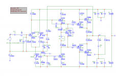
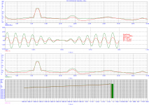
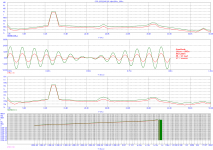
Here is an IMD analysis of the plain P3A and my circuit. I have also run a few IMD analysis of some modified P3A circuit, It was surprising though that none comes closer to the plain P3A and simulation shows that currents and voltages of these circuit is almost identical to that of the plain P3A.
@mosquito,
I have tried that technique before in the VHex thread. You can pm me your simulated circuit.")
@Andrew T,
VAS current is at 6ma. Your suggestion of the 8.2k with an e-cap to ground looks like the Blameless approach.
Here is an IMD analysis of the plain P3A and my circuit. I have also run a few IMD analysis of some modified P3A circuit, It was surprising though that none comes closer to the plain P3A and simulation shows that currents and voltages of these circuit is almost identical to that of the plain P3A.
@mosquito,
I have tried that technique before in the VHex thread. You can pm me your simulated circuit.
@Andrew T,
VAS current is at 6ma. Your suggestion of the 8.2k with an e-cap to ground looks like the Blameless approach.
Attachments
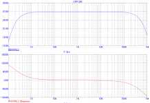
^at that frequency even the board lay-out will have an effect even if you can get to make that smooth in simulations.....
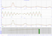
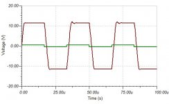
that "horn" at the top swing is called overshoot, frequency compensation ought to take care of that...exactly how? that is the exciting part, i am sure the gurus here will chime in..
how do the waveform look like at 10khz? square wave testing at 100hz, 1 khz and 10khz are usually enough...
that "horn" at the top swing is called overshoot, frequency compensation ought to take care of that...exactly how? that is the exciting part, i am sure the gurus here will chime in..
how do the waveform look like at 10khz? square wave testing at 100hz, 1 khz and 10khz are usually enough...
- Home
- Amplifiers
- Solid State
- P3A-More upgrades