DouglasSelf said:
As to the first question, I think that in an EF output stage the driver dissipation varies much less with output level than it does in the output devices, (see Fig 13.1 in the 4th edition of Audio Power Amplier Design) so it should be much less of a problem.
Not quite sure I understand the second question. Are you saying that the diode tempco will vary with the current through it? Apart from anything else, Bob Cordell's graph (which I take the liberty of attaching) says otherwise.
Douglas
1. Yes the tempco of the diode is changing with the current see post 127 and following in B cordell thread on thermaltrack.
I derived this simple equation:
tempco variation = k/q * ln ( I2/I1) where k/q = 0.086 mV/°K
this gives the usefull rule of thumb :
tempco variation = - 0.2mV/°C per decade decrease of current
The graph from B. Cordell do not show it because you need at least a decade of current drop.
If you look at the thermaltrack spec ( last figure) the diode tempco variation can be estimated and is 0.2 mV/°C for a decade drop of current
2. Then by bleeding current from the diode you adjust the tempco.
The Vbe of the diode with bias current is irrelevant because you can get the right bias in a Vbe multiplier by adjusting the multiplier factor.
Having the diodes in the upper leg of the base and the Vbe multiplier potentiometer in the lower leg allows to design and tune for the optimal bias at room temperature.
Then by adjusting the // resistors on each couple of diodes you can adjust the tempco of the diodes to have a better tracking
3. Large transient T° mistraking of output transistor Vbe will create evidently bursts of crossover distortion due to transient under or over bias. This is a non linear phenomenon difficult to model and to measure but we know it exists.
With the help of Thermaltracks, we can have a by fare better temperature tracking. Then the question arise: what tempco to utilise and how?
In the other thread, the thermaltracks where criticized because their tempco is not the same as the Vbe tempco of the ouput transistors. By adjusting the current in the diodes, you can tune the tempco to the exact value required.
Would this be optimal? No
In your book you gave the optimal Vq of about 26mV. In Oliver's paper ( I got the reference from your book thanks ! ) it is shown that the optimal bias is for :
gm* R = 1 this means Io * R = Vt = 26mV at room temp !!!!
where R is the resistance looking in the emitter of one transistor at bias, Io is the bias current and Vt is tehe thermal voltage.
Io * R is also your Vq if R is dominated by the emitter resistor.
This shows that at high temperature, the Vq so Io should rise to maintain optimal bias. This is of course a secondary effect but if we can get a good thermal tracking, then it may become a first order effect certainly at the low currents where crossover happens
3. Conclusion
By tuning the Vbias at room temperature for minimum distortion ( using a spectrum analyzer ). Then tuning the diodes tempco to minimize the distortion at high temperature, we can have a better amplifier.
The only reactions I had were from B. Cordell and Janneman. Thanks to them !!
I can be wrong but it seams that people are more interested in sophisticated circuit topologies or defending strange third order phenomena like cables, jfets and so on.
I am interested by your opinion on the reality of this. I hope to be able to measure and apply thsi in a near future.
JPV
variation of diode VF tempco with bias current
Reading the Thermaltrack transistors NJL3281D spec, fig 15 diode forward voltage/
at 1 Amp Vf = 0.93 V at -25°C
Vf = 0.75 V at 100°V
then tempco at 1 Amp = (0.75-0.93)/125 = -1,44 mV/°C
at 1mA Vf = 0.59 V at -25°C
Vf = 0.34 v at 100°C
then tempco at 1mA = ( 0.34 - 0.59) /125 =- 2mV
Delta tempco = - 0,56mv/°C for 3 decades of current
This is about -0.2mV/°C per decade of current
JPV
A colleague of mine made a nice video on crossover distortion change with load (temperature). He prepared optimally biased class B, with quite right thermal coupling of Vbe multiplier. He measured on oscilloscope screen, with fundamental notched. Changed load in sudden steps, i.e. changed tepmerature dynamically. One could see slowly changed crossover residual. To me, class B would never hit optimum, for many reasons.
PMA said:
... optimally biased class B, with quite right thermal coupling of Vbe multiplier. He measured on oscilloscope screen, with fundamental notched. Changed load in sudden steps, i.e. changed tepmerature dynamically. One could see slowly changed crossover residual. To me, class B would never hit optimum, for many reasons.
Hi Pavel
It is not the same case as if you have a thermal tracking jonction insight the power BJTs.
But you might be right ... at step response the thermal tracking Vbe monitoring device will respond with some lag. On the other hand, there is no step like change in the normal audio signal, so a device with a monitoring diode very close to his BE junction will provide a minimal lag between audio signal and Vbe thermal correction signal.
Cheers,
Mihai
PMA said:A colleague of mine made a nice video on crossover distortion change with load (temperature). He prepared optimally biased class B, with quite right thermal coupling of Vbe multiplier. He measured on oscilloscope screen, with fundamental notched. Changed load in sudden steps, i.e. changed tepmerature dynamically. One could see slowly changed crossover residual. To me, class B would never hit optimum, for many reasons.
We all know that crossover is changing with temperature.
The point is " quite right thermal coupling ". How was it done without on the chip sensor.
You do not give any technical comment on the content of my post.
By paralleling many ouput transistors optimally biased even in a transient way we could reach very good performance where the crossover distortion vanishes or at least be very low.
JPV
PMA said:A colleague of mine made a nice video on crossover distortion change with load (temperature). He prepared optimally biased class B, with quite right thermal coupling of Vbe multiplier. He measured on oscilloscope screen, with fundamental notched. Changed load in sudden steps, i.e. changed tepmerature dynamically. One could see slowly changed crossover residual. To me, class B would never hit optimum, for many reasons.
I think you missed the point of JPV's post. He argues that it is possible to all but eliminate that thermally-induced operating point transient due to sudden load changes.
What do you think of his reasoning?
Jan Didden
PMA said:Similar (i.e. that long one), but not absolutely same in response as sense/FB circuit.
But the sensor is on the same die. If you don't know what the numbers are, how can you know they are different and how long they actually are?
What happened to your sharp reasoning mind?
And of course that 17uS is nonsense.
Jan Didden
janneman said:But the sensor is on the same die. If you don't know what the numbers are, how can you know they are different and how long they actually are?
What happened to your sharp reasoning mind?
And of course that 17uS is nonsense.
Jan Didden
Jan, from the other thread, somebody mentioned a run of devices that had the incorrect diode put in. That would mean the die is an independent descrete device..
From the junction to the bottom of the die, a typical number I've seen used for transient thermal is 100 uSec to 1 milli. Junction to case was in the 10 to 100 mSec. For a die that is epoxy bonded to the top of a bipolar junction, I'd expect the time constant to be in the 10 to 100 millisecond range.
It's easy enough to check, why hasn't anybody done so?
Cheers, John
anatech said:Hi Douglas,
One manufacturer I know of used glass signal diodes between the C and E leads on the driver transistors. In this way they could track the die temperature better in the driver stage. A little heat sink grease blocked air currents from altering the temperature of the signal diodes. The Vbe multiplier transistor was mounted on the heat sink between the output devices.
From what I have seen in service, a slight overcompensation for bias control seems to work the best. Some of this is related to the heat sink size and air flow also. So an over compensated amp on my bench may well be under compensated in the customer's set up. Even the top cover position will change the bias tempco as everything else runs warmer with the top on.
I raise these points because we tend to talk about output circuitry in isolation when in fact we need to consider the entire system. In this case, all changes in the circuitry operation due to temperature rise. This can easily take a critically compensated output stage and turn it into a thermal runaway victim. I have seen this too many times over the years.
-Chris
Hi Chris
That's a most interesting idea. Am I right in thinking that the idea is to sense the temp of the collector lead, because that will be directly connected to the metal area on the package?
I have only seen one case of thermal runaway in decades of amplifier work. I think you would need a seriously under-sized heatsink for it to happen. My last commercial design had the sensor on the drivers rather than the main heatsink (for reasons I won't bore you with) which may not be ideal, but in severe testing there was never a hint of runaway- and that was with the additional heating from Class-XD operation.
Douglas
posted by douglasself..I have only seen one case of thermal runaway in decades of amplifier work. I think you would need a seriously under-sized heatsink for it to happen
I think you have described most HT receivers on the market
today!
 (thank god they have thermal cutoff in their protection circuits) .
The idea of putting the Vbe on the collector leg is cool

I'll try it.(poor mans way of getting thermaltrak performance)
BTW.. Thanks,Mr. Self, for the BEST book on amplifier design
and for the "blameless design" which with proper layout
and device selection is one killer amp. I look forward to the latest
edition (I only have Ed.3).
Thanks,OS
JPV said:
1. Yes the tempco of the diode is changing with the current see post 127 and following in B cordell thread on thermaltrack.
I derived this simple equation:
tempco variation = k/q * ln ( I2/I1) where k/q = 0.086 mV/°K
this gives the usefull rule of thumb :
tempco variation = - 0.2mV/°C per decade decrease of current
The graph from B. Cordell do not show it because you need at least a decade of current drop.
If you look at the thermaltrack spec ( last figure) the diode tempco variation can be estimated and is 0.2 mV/°C for a decade drop of current
2. Then by bleeding current from the diode you adjust the tempco.
The Vbe of the diode with bias current is irrelevant because you can get the right bias in a Vbe multiplier by adjusting the multiplier factor.
Having the diodes in the upper leg of the base and the Vbe multiplier potentiometer in the lower leg allows to design and tune for the optimal bias at room temperature.
Then by adjusting the // resistors on each couple of diodes you can adjust the tempco of the diodes to have a better tracking
3. Large transient T° mistraking of output transistor Vbe will create evidently bursts of crossover distortion due to transient under or over bias. This is a non linear phenomenon difficult to model and to measure but we know it exists.
With the help of Thermaltracks, we can have a by fare better temperature tracking. Then the question arise: what tempco to utilise and how?
In the other thread, the thermaltracks where criticized because their tempco is not the same as the Vbe tempco of the ouput transistors. By adjusting the current in the diodes, you can tune the tempco to the exact value required.
Would this be optimal? No
In your book you gave the optimal Vq of about 26mV. In Oliver's paper ( I got the reference from your book thanks ! ) it is shown that the optimal bias is for :
gm* R = 1 this means Io * R = Vt = 26mV at room temp !!!!
where R is the resistance looking in the emitter of one transistor at bias, Io is the bias current and Vt is tehe thermal voltage.
Io * R is also your Vq if R is dominated by the emitter resistor.
This shows that at high temperature, the Vq so Io should rise to maintain optimal bias. This is of course a secondary effect but if we can get a good thermal tracking, then it may become a first order effect certainly at the low currents where crossover happens
3. Conclusion
By tuning the Vbias at room temperature for minimum distortion ( using a spectrum analyzer ). Then tuning the diodes tempco to minimize the distortion at high temperature, we can have a better amplifier.
The only reactions I had were from B. Cordell and Janneman. Thanks to them !!
I can be wrong but it seams that people are more interested in sophisticated circuit topologies or defending strange third order phenomena like cables, jfets and so on.
I am interested by your opinion on the reality of this. I hope to be able to measure and apply thsi in a near future.
JPV
Hi JPV, sorry I couldn't get back to you yesterday.
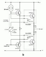
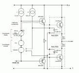
My first attempt at applying the ThermalTraks was to assume that the diodes would be used to attempt to directly cancel the transistor Vbe voltages,which means running the diodes at 25 mA (for transistor Ic=100mA) and accepting that the tempco would not match exactly. The compensation should, I think, still be much better than conventional methods but it is certainly not theoretically perfect. This is the approach I used in the attached circuit, which I think of as Plan A. I have never tried to run a VAS at 25 mA,and I fear the linearity might be worse. Certainly TO-92 transistors will get too hot for amplifiers above 100W/8R, which is a problem as the bigger devices tend to have less beta. A VAS buffer may be needed.
I accept what you say about increasing diode tempco's by reducing the current. I have just reread RA Pease's thoughts on it; http://www.national.com/rap/Story/vbe.html and and he certainly quotes - 0.2mV/°C per decade decrease of current. Our diodes have a tempco of 1.7 mV/degC and the transistor Vbe has a tempco of 2.14 mV/degC at 25mA (Bob Cordell's figures) so diode tempco needs to be increased by 0.44 mV/degC. The diode current therefore needs to reduced by 2.2 decades, or 158 times. That gives us a diode current of 158 uA. (not a typo) This is much too low for a VAS operating current so we need a circuit that will replicate the diode voltage at much greater current.
The lower current is clearly not going to give us enough diode voltage to cancel the transistor Vbe's directly. However we cannot use a conventional multiplier circuit as in multiplying the voltage we also multiply the tempco. What is needed is to add a fixed voltage to the diode voltage. If we assume we are using an EF type 2 output, then we also need compensation for the driver Vbe's which can be done with a conventional Vbe multiplier circuit, as used in Plan A.
Another point is that a diode current of 158 uA is quite small, and whatever circuitry we use will have to have its base currents looked at carefully if it is not be inaccurate.
It therefore looks as if we need a system like that shown conceptually in the second diagram. Vdriver compensates the driver Vbe's. The fixed voltage is derived from black box called Vfix, and the diode voltages are replicated by a black box called Vdiodes. I am calling this approach Plan B. It should give much better compensation than Plan A, but it's going to take a bit of designing...
What do people think?
I'm not sure if I can put two pictures in one post, but I'm about to find out.
Douglas
Attachments
But if we put the diodes in the upper leg of the Vbe multiplier base circuit (like leach) their tempco won't be multiplied. And 160µA sounds like a reasonable current to have flowing there, just use a buffer for the Vbe multiplier transistor and it will have enough beta to be stable with vas current.
Or is your worry that when doing this the tempco of the vbe multiplier transistor part will be too high, decreasing idle current with increased ambient/driver temperature? But this should be pretty stable.
edit:
"But this should be pretty stable." was referring to the ambient temperature which won't vary as much as output transistor case temperature.
Re: Re: Re: do we need stable bias current with temp in the output stage? NO
Hello Douglas
I alway use EF output stage in my diy amps and I use oversize heasink for the drivers, so the dissipation on the drivers varies much less, in that way I only thermally couple the transistor in the Vbe multiplier to the output transistors.
Thank
Bye
Gaetan
DouglasSelf said:
Hi Gaetan
I had a quick look at this circuit today, and I'm not sure it will do the job. The current through the diodes is only 1.2 mA, and their voltage drop (which with this circuit is simply added to the output voltage, and not multiplied in any way) will therefore be much too low to cancel the output device Vbe's. Bob Cordell's figures show that 25 mA gives a good match for 100mA in the outputs.
Minimum output voltage is 4.13V, which seems too much; that's seven Vbe's.
Presumably the transistor in the Vbe multiplier is thermally coupled to the drivers? You mentioned something about two more diodes, so I may have that wrong.
Douglas
Hello Douglas
I alway use EF output stage in my diy amps and I use oversize heasink for the drivers, so the dissipation on the drivers varies much less, in that way I only thermally couple the transistor in the Vbe multiplier to the output transistors.
Thank
Bye
Gaetan
- Status
- This old topic is closed. If you want to reopen this topic, contact a moderator using the "Report Post" button.
- Home
- Amplifiers
- Solid State
- On Semi ThermalTrak