DouglasSelf said:The question was asked a while back as to how the response of the internal diode compared with the temperature rise on the top of the package. (Which has I think now been demonstrated to definitely be the best sensor position for non-TTrak transistors)
Time for a Yuletide experiment. In the attached screen-shot the diode voltage for a 5mA current is at the top, and the lower trace is the temperature at the top of the package as measured by an LM35 TO-92 temp sensor. Assuming -2mV/degC for the diode, both scales are 5 degC per large division. The power step was 6W, TTrak was on a sizable heatsink, thermal washer Koolpad K230 fitted between the TTrak top and the LM35.
The internal diode responds more and faster, no question there. Hmm!
Am I missing something, because I don't find this surprizing. I don't agree with what has been said about the internal diode being "out of the thermal path". Heat will flow from hot to cold, and flow faster along a conductor than an insulator. So what's the surprize? The internal diode is mounted on the same conductor as the transistor junction. Heat is not going to choose a different path. It will flow where there's a differential.
I have been using the NJL3281D/1302D and in simulation couldn't find a good fit diode model (wound up using some 1N4001 with some MUR1520). Your model is an exact match for the real performance I'm seeing with the actual amp.
MJL,
Be careful. The model I posted is for the diode in the 4xxx series. The diode in the 3xxx is different. I'll play around and see how close the 3281 model is to reality and tweak that one too...
John
jgedde said:
MJL,
Be careful. The model I posted is for the diode in the 4xxx series. The diode in the 3xxx is different. I'll play around and see how close the 3281 model is to reality and tweak that one too...
John
Hi John,
The model must be close at my VAS current (3mA). Simulation is giving me the same results now as the measurements from the actual, real, built and functioning amp.
")
Attachments
pooge said:
Am I missing something, because I don't find this surprizing. I don't agree with what has been said about the internal diode being "out of the thermal path". Heat will flow from hot to cold, and flow faster along a conductor than an insulator. So what's the surprize? The internal diode is mounted on the same conductor as the transistor junction. Heat is not going to choose a different path. It will flow where there's a differential.
I tend to agree. The copper header will tend to have fairly low thermal gradient anyway. Although it is not perfectly isothermal, I think differentials across it will be fairly small. In my model above, I assumed a total of only 0.1C/W from the bottom of the die to the back of the case. I did allow 0.03C/W of that as a local header thermal resistance right under the die because of the concentration of heat input there.
Cheers,
Bob
Bob Cordell said:
I tend to agree. The copper header will tend to have fairly low thermal gradient anyway. Although it is not perfectly isothermal, I think differentials across it will be fairly small. In my model above, I assumed a total of only 0.1C/W from the bottom of the die to the back of the case. I did allow 0.03C/W of that as a local header thermal resistance right under the die because of the concentration of heat input there.
Bob,
The diode is mounted (on the common copper plate) isolated using epoxy. It is the epoxy (relative) poor thermal conductivity and the diode chip thermal mass that creates the temperature gradient between the transistor and the diode chips, under transient conditions.
Under thermal equilibrum conditions (which maps to the static bias conditions of the output stage), I agree that the temperatures of the transistor and diode chips are very close. Though, it is my understanding we are discussing here the dynamic regime, where things are barely at thermal equilibrum.
DouglasSelf said:The question was asked a while back as to how the response of the internal diode compared with the temperature rise on the top of the package. (Which has I think now been demonstrated to definitely be the best sensor position for non-TTrak transistors)
Time for a Yuletide experiment. In the attached screen-shot the diode voltage for a 5mA current is at the top, and the lower trace is the temperature at the top of the package as measured by an LM35 TO-92 temp sensor. Assuming -2mV/degC for the diode, both scales are 5 degC per large division. The power step was 6W, TTrak was on a sizable heatsink, thermal washer Koolpad K230 fitted between the TTrak top and the LM35.
The internal diode responds more and faster, no question there. Hmm!
Hi Doug,
Nice work. If I'm interpreting your time scale correctly, (5 sec/div), it looks like the thermal time constant of the transistor/header assembly, in connection with the thermal resistance from case to heat sink, is about 20 seconds. I'm assuming the heat sink is fairly large, and doesn't move much thermally. What do you estimate the thermal resistance from case to sink is in your experiment?
In experiments I did yesterday, I wanted to measure the thermal mass of the transistor/header. I put in 12 watts and estimated that the thermal resistance from case to sink was about 0.7 C/W (not a great contact). The heat sink was large.
I then looked at the thermal time constant of the diode's response and got about 7 seconds. This all implied to me that the thermal capacity was larger than what I had assumed in my model above. By these measurements, the total thermal capacity was estimated to be on the order of 9.6 Farads.
I next dis-mounted the transistor from the heat sink and measured the thermal slew rate of the transistor body, as implied by the rate of change of the temperature seen by the diode. I assumed 1.7 mV/C for the diode. In this situation, the only shunting thermal resistance would be the thermal resistance from package to ambient, so the behavior should largely be like an integrator.
The diode voltage slewed 20 mV in 8 seconds, implying a temperature slew rate of 1.47 C/second. With a 12 watt input, the thermal capacitance by this method is estimated to be about 8.2 Farads in my model.
These two numbers seem reasonably close to each other, given the two different techniques and all the assumptions and potential innaccuracies involved.
Bottom line seems to be that the thermal time constant of the transistor/header mounted typically on a large heat sink seems to be 5 seconds or more, as contrasted with the 1 second I assumed earlier.
Cheers,
Bob
syn08 said:
Bob,
The diode is mounted (on the common copper plate) isolated using epoxy. It is the epoxy (relative) poor thermal conductivity and the diode chip thermal mass that creates the temperature gradient between the transistor and the diode chips, under transient conditions.
Under thermal equilibrum conditions (which maps to the static bias conditions of the output stage), I agree that the temperatures of the transistor and diode chips are very close. Though, it is my understanding we are discussing here the dynamic regime, where things are barely at thermal equilibrum.
Hi syn08,
I have thought about the thermal resistance of the insulating diode die attach and the thermal mass of the diode die. Perhaps wrongly, I dismissed it as a significant factor. The epoxy layer attaching the die is very thin, and the diode die mass is quite small, so I guessed that the thermal time constant there would be small compared to the several-second time constant of the copper header.
Have you got some calculations or measurements that would allow us to estimate the thermal time constant of the diode/header interface?
Thanks,
Bob
jgedde said:Here's a PSPICE model for the diode in the 4xxx that I tweaked to reflect reality. This model is for 27 degC only as I haven't been able to tweak the model sucessfully to model its behavior over temperature. I gave up on that...
.MODEL Dnjl4302dg_diode d
+ IS=5.5e-008 RS=0.65 N=2 TT=5.1937e-008 CJO=2.08272e-011 VJ=1.5+/n M=0.653713 EG=1.3 XTI=2.33354 BV=400 IBV=1e-005
John
John, thanks for this model and all of the work you have done here. Awhile back I did a very poor-man's tweak of the diode model for the NJL3281, but it was just to get by with. I've been taking some data to come up with a better one for the 3281, so this should be a good start for that device.
Thanks again,
Bob
Bob Cordell said:
Have you got some calculations or measurements that would allow us to estimate the thermal time constant of the diode/header interface?
I have a ballpark calculation, from the top transistor chip (where heat is generated) to the top of the diode chip (where the temperature is to be tracked). I'll be back after Xmas.
Bob Cordell said:
Hi Doug,
Nice work. If I'm interpreting your time scale correctly, (5 sec/div), it looks like the thermal time constant of the transistor/header assembly, in connection with the thermal resistance from case to heat sink, is about 20 seconds. I'm assuming the heat sink is fairly large, and doesn't move much thermally. What do you estimate the thermal resistance from case to sink is in your experiment?
In experiments I did yesterday, I wanted to measure the thermal mass of the transistor/header. I put in 12 watts and estimated that the thermal resistance from case to sink was about 0.7 C/W (not a great contact). The heat sink was large.
Hi Bob
Quick answer in between excessively large meals.
The time scale was indeed 5 sec/div. Heat sink large enough to alter very little on this time scale.
Thermal resistance from case to sink calculates as 0.77 degC/W but probably a bit higher as mounting pressure low to avoid crushing the LM35.
DouglasSelf said:
Hi Bob
Quick answer in between excessively large meals.
The time scale was indeed 5 sec/div. Heat sink large enough to alter very little on this time scale.
Thermal resistance from case to sink calculates as 0.77 degC/W but probably a bit higher as mounting pressure low to avoid crushing the LM35.
Hi Doug,
Thanks. It sounds like our observations are reasonably in the same ballpark, namely that the thermal time constant of the transistor/header assembly, when interfaced to a heat sink, is considerably more than one second.
I have also been eating too much
.Happy Holidays,
Bob
thanh1973 said:Would it be easy to incorporate these thermaltraks into a naim clone design?
If so would the results be worth it (The Naim design is prone to thermal runaway if biasing to high)?
I can supply a schematic if required.
If you can show me the circuit I'll give it some thought.
Bob Cordell said:
Hi Doug,
Thanks. It sounds like our observations are reasonably in the same ballpark, namely that the thermal time constant of the transistor/header assembly, when interfaced to a heat sink, is considerably more than one second.
I have also been eating too much
Happy Holidays,
Bob
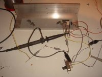
Yes, much more than a second. The test I did on Xmas Eve shows that the diode voltage took 29.5 seconds to reach 63% of its final value. I must admit that is a lot slower than I expected.
Attached is a pic of the experimental setup so you can see the heatsink size. Not exactly the Large Hadron Collider, but I think it did the job.
Attachments
Hi Bob
Some proper information on the heatsink I used:
Volume (measured) 100,392 mm3
Mass (calc'd) 271 gms
Heat capacity (calc'd) 244 J/degC
Thermal resistance to ambient- heaven knows, but I am guessing about 5 degC/W
I hope these look like reasonable figures to you. I have been trying to put together an RC thermal model using some of the figures for internal thermal resistance & capacity discussed in this thread and obtained elsewhere, and it's not going well, with figures from different sources varying by orders of magnitude. How are you doing with that?
Thermaltraks for Naim Clone Design
Hi Doug
Here is the schematic
Thanks
There are a couple of mistakes on this schematic (ie things left out).
On the +ve and -ve power rails there should be a diode (1N4004) and a 330 ohm resistor (ie going from right to left) between supplying the driver transistors (MJE15032, MJE15033) and supplying ZTX753/653 transistors.
There should also be 100 ohm emiter resistors on the LTP (2sc2547E).
I am not sure if this information is realy necessary but I thought I should include it for completeness.
Attachments
Re: Thermaltraks for Naim Clone Design
Hmmm. Not exactly state of the art, eh?
The problem here is that the output stage is a quasi-complementary type, so the bias compensation requirements for the top & bottom halves will be completely different. If you want to apply TTrak transistors, I'm afraid this looks like a really bad place to start.
thanh1973 said:Hi Doug
Here is the schematic
Thanks
There are a couple of mistakes on this schematic (ie things left out).
On the +ve and -ve power rails there should be a diode (1N4004) and a 330 ohm resistor (ie going from right to left) between supplying the driver transistors (MJE15032, MJE15033) and supplying ZTX753/653 transistors.
There should also be 100 ohm emiter resistors on the LTP (2sc2547E).
I am not sure if this information is realy necessary but I thought I should include it for completeness.
Hmmm. Not exactly state of the art, eh?
The problem here is that the output stage is a quasi-complementary type, so the bias compensation requirements for the top & bottom halves will be completely different. If you want to apply TTrak transistors, I'm afraid this looks like a really bad place to start.
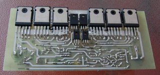
jgedde said:I forgot I had a camera in my phone! Sorry about the poor quality (no macro), but you get the idea...
John
Hi John
Could you tell us how thick the copper header is? I'm trying to put together a thermal model that matches the tests I did on Xmas Eve.
One again many thanks for all your hard work.
Bob Cordell said:
In experiments I did yesterday, I wanted to measure the thermal mass of the transistor/header. I put in 12 watts and estimated that the thermal resistance from case to sink was about 0.7 C/W (not a great contact). The heat sink was large.
I then looked at the thermal time constant of the diode's response and got about 7 seconds. This all implied to me that the thermal capacity was larger than what I had assumed in my model above. By these measurements, the total thermal capacity was estimated to be on the order of 9.6 Farads.
I next dis-mounted the transistor from the heat sink and measured the thermal slew rate of the transistor body, as implied by the rate of change of the temperature seen by the diode. I assumed 1.7 mV/C for the diode. In this situation, the only shunting thermal resistance would be the thermal resistance from package to ambient, so the behavior should largely be like an integrator.
The diode voltage slewed 20 mV in 8 seconds, implying a temperature slew rate of 1.47 C/second. With a 12 watt input, the thermal capacitance by this method is estimated to be about 8.2 Farads in my model.
These two numbers seem reasonably close to each other, given the two different techniques and all the assumptions and potential innaccuracies involved.
Bottom line seems to be that the thermal time constant of the transistor/header mounted typically on a large heat sink seems to be 5 seconds or more, as contrasted with the 1 second I assumed earlier.
Cheers,
Bob
Hi Bob
I now have a crude thermal model which correlates with the diode temperatures in the LM35 experiment. I have assumed that the die and solder heat capacities are negligible compared with the copper header capacity and that the copper thermal resistance is very low, so that almost all the spec'd thermal resistance junction-to-case (0.694 degC/W) is in the die and solder.
Working empirically from the time/temp curve I get 8.0 J/degC as the header thermal capacity, which is very close to your figure. So far so good.
We know the area of the header (318 mm2) so we can work out the depth of the header that would give 8.0 J/degC. The answer I get is 7.2mm, which is rather regrettably greater than the thickness of the whole package. (5mm)
Clearly something is amiss. Adding the thermal capacity of the plastic doesn't look like it will fix it. Any thoughts?
- Status
- This old topic is closed. If you want to reopen this topic, contact a moderator using the "Report Post" button.
- Home
- Amplifiers
- Solid State
- On Semi ThermalTrak