Hi all,
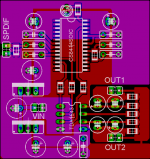
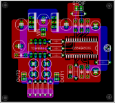
I've attached some pics of my PCB layout for a planned TDA1543 DAC. I am using a CS8414 reciever following the standard non-os trend. The schematics are basically the same as Fedde's NONOZ III design: jwg.student.utwente.nl/fedde/nonoz3.html
The plan is to use the bottom of the board as the power ground and the top as the digital ground. You will see in the picture that the power components are not isolated from the digital ground in the top layer. This won't be a problem as I am not using plated through holes since I am etching the boards myself. the two ground planes will connect at the power supply connection.
My plan is to mate this with a PCM2906 or 2706 USB DAC, and an OPA627/Buf634 preamp that I have already completed.
Any comments or suggestions are very welcome, as this is only my second digital design.
G.
Attachments
You may want to leave yourself a possible connection between grounds right at the DAC, instead of at power supplies. Separate grounds can be a very dangerous thing, having exactly the opposite effect intended.
Look at the return current paths for every signal. My concern here are the digital lines between receiver and converter. Just where does the return path go? You have these very fast transient edges going direct from one chip to the other, then a return current going way out to the edge of the board and back. This is a discontinuity and forms a large inductive loop and crosstalk. There are also connections within the converter chip itself (it helps to have a complete schematic of the innards of each chip) passing transient signals from one ground system to another. These transients have no local return path, hence inducing glitches right where you thought you got rid of them.
IMHO, the best place to connect different ground & supply systems is right where the two meet, under the converter chip.
jh")
Look at the return current paths for every signal. My concern here are the digital lines between receiver and converter. Just where does the return path go? You have these very fast transient edges going direct from one chip to the other, then a return current going way out to the edge of the board and back. This is a discontinuity and forms a large inductive loop and crosstalk. There are also connections within the converter chip itself (it helps to have a complete schematic of the innards of each chip) passing transient signals from one ground system to another. These transients have no local return path, hence inducing glitches right where you thought you got rid of them.
IMHO, the best place to connect different ground & supply systems is right where the two meet, under the converter chip.
jh
Some suggestions: Implement the option for an input transformer. Edit the layout so that film caps can be used at the output. Break the loop in the groundplane above the input caps. Add some extra SMD caps right at the supply pins of CS8414. Maybe you can add the sin x/x rolloff filter ??
Personally I would not design the board for SMD resistors only as normal metal film ones sound better and availability is no problem.
Looks good !
Personally I would not design the board for SMD resistors only as normal metal film ones sound better and availability is no problem.
Looks good !
Jean-Paul/Hagtech
Wow, thanks so much for the suggestions. This is the kind of help I was looking for. I'm quite the noob when it comes to digital design...I'm sure it shows.
Hagtech, as for the connection between the grounds, shoul this be at the supply from the DAC (this is already pretty much the central ground point, or should it be at the output? I will make an attempt to reduce the size of the groundplane to shorten the return paths as much as possible.
Jean-Paul, could you be a bit more specific as to the "loop in the groundplane above the input caps". I'm looking but I don't see it??? I do se that I broke the power ground at the SPDIF input, I will fix this later tonight.
What are your thoughts on star grounding. Would I really be better off with just a single ground rather than making any attempt to keep them seperate?
Thanks
G.
I haven't looked at the layout ... But in general, if you choose to use two ground sections, tie them together at the DAC. Not at output connectors or power supply connectors.
Start grounding is great, if done right. Not as simple as it sounds. ALL signals and ALL supplies must use the same star. Otherwise benefits are lost. Makes things more difficult.
jh
Start grounding is great, if done right. Not as simple as it sounds. ALL signals and ALL supplies must use the same star. Otherwise benefits are lost. Makes things more difficult.
jh
hagtech said:
Look at the return current paths for every signal.
jh
Yes, yes, yes ! Think in current loops guys, Kirchoff must have an internet connection somewhere, so watch out .......
http://www.tentlabs.com/Info/Articles/Supply_decoupling.pdf
best
May a good thing to ask here:
My CDP has a groundplane (Philips CD660 and others), and the circuit uses several conecting points on that groundplane to connect parts to gnd, these points are spreaded on several places of whole groundplane. My idea is to isolate those connections, and choose ONE star-point (near dac) and connect all the ground conections from there with massive 1.5 gauge wire.
Wil this improve grounding layout?
Thanks!
tubee said:May a good thing to ask here:
My CDP has a groundplane (Philips CD660 and others), and the circuit uses several conecting points on that groundplane to connect parts to gnd, these points are spreaded on several places of whole groundplane. My idea is to isolate those connections, and choose ONE star-point (near dac) and connect all the ground conections from there with massive 1.5 gauge wire.
Wil this improve grounding layout?
Thanks!
Hi
No it won't, someone suggested to look at the current loops.....
Attaching them to several places to the plane isn't a problem as long as no big (RF) currents flow through the plane. To avoid that, several suggestions are given in my article.
best
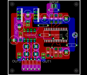
TDA1543 REVB
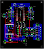
Alright, I decided to try and star ground this thing. I also opted to use through hole resistors rather than SMD. Not because of the quality point, but because it makes it easier to couple traces between top and bottom.
You will see that the central ground is at the DAC. The routing gets a bit messy, so if you can see a way to shorten some of the traces let me know. I tied AGND and DGND of the CS8418 together beneath the chip...will this present a problem or do I need to keep them seperate until they meet at the central ground point?
The dimensions of the board are 2.5" x 2.25"
Anxiously awaiting your suggestions
G.
Attachments
I think this is going to be too hard to explain. If you can't visualize the induced electric and magnetic fields in four dimensions, you're not going to get what I'm trying to say. Or perhaps, it's just my inability to translate things into words. It's a visual thing.
The board is all wrong. I apologize for having to say that, but assume you would prefer honesty.
A good example is C4. This is probably the loop filter cap for the PLL. It needs to be tied right back the the analog ground pin of the chip. Not somewhere else on the board. You've got crosstalk everywhere.
My advice for such a small board, is to just run a ground plane under the whole thing. You'll have better luck.
jh
hagtech said:I think this is going to be too hard to explain. If you can't visualize the induced electric and magnetic fields in four dimensions, you're not going to get what I'm trying to say. Or perhaps, it's just my inability to translate things into words. It's a visual thing.
The board is all wrong. I apologize for having to say that, but assume you would prefer honesty.
A good example is C4. This is probably the loop filter cap for the PLL. It needs to be tied right back the the analog ground pin of the chip. Not somewhere else on the board. You've got crosstalk everywhere.
My advice for such a small board, is to just run a ground plane under the whole thing. You'll have better luck.
jh
Hey, honesty is good! If you are not going to give your honest opinion, then I will totally waste my time in building something that doesn't work as it should. While I'm not looking to build "The Ultimate" DAC I would like something descent. I'll make a few more changes and see what your thoughts are.
Thanks!
Stick with wide ground traces. Or make it a plane. Your circuit should actually work as-is, but will have excess jitter and glitches and noise in the output that don't deserve to be there.
I recently did the same circuit (almost). Ground plane is best way to go for the high speed stuff, and then you section things off. I put digital on left, converter in middle, output on right. No crossing or mixing of signals. I don't run any digital traces across the analog, or vice versa.
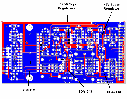
I tried to use same colors as you did. Blue is all ground. Hard to see, but I have decoupling caps right on the pins they need to be with returns as short as possible.
I know you're just starting out as a layout designer. Hang in there. We all learn the hard way. There's just no way I can condense 20 years of this into a few paragraphs.
jh
I recently did the same circuit (almost). Ground plane is best way to go for the high speed stuff, and then you section things off. I put digital on left, converter in middle, output on right. No crossing or mixing of signals. I don't run any digital traces across the analog, or vice versa.
I tried to use same colors as you did. Blue is all ground. Hard to see, but I have decoupling caps right on the pins they need to be with returns as short as possible.
I know you're just starting out as a layout designer. Hang in there. We all learn the hard way. There's just no way I can condense 20 years of this into a few paragraphs.
jh
Advisable PCB solutions
I am going to design a PCB for a CS8412 + TDA1541 DAC. I can only manage a double sided PCB for a two layer routing (no internal layers).
I have two ideas:
First idea
Use bottom layer for all connections. Analog ground connections and digital ground connections use a bus schema (two separate buses).
Use top layer as a ground plane, insulated from all components. The ground plane on top is connected, in a single point, to the analog and digital ground buses on the bottom layer.
Second idea
Use top layer as a ground plane, analog and digital ground connections directly soldered as they are on the components; so ground connections spread all over the plane and there is no separation between analog and digital ground.
Use bottom layer for all the remaining connections.
Are these "good" ideas? And if yes, which is better?
What about swapping the side role (i.e. ground plane on the bottom layer) ?
I'd greatly appreciate suggestions from you skilled friends (I am an absolute beginner...)
Best regards.
Paul
hagtech said:Stick with wide ground traces. Or make it a plane. Your circuit should actually work as-is, but will have excess jitter and glitches and noise in the output that don't deserve to be there.
I recently did the same circuit (almost). Ground plane is best way to go for the high speed stuff, and then you section things off. I put digital on left, converter in middle, output on right. No crossing or mixing of signals. I don't run any digital traces across the analog, or vice versa.
I tried to use same colors as you did. Blue is all ground. Hard to see, but I have decoupling caps right on the pins they need to be with returns as short as possible.
I know you're just starting out as a layout designer. Hang in there. We all learn the hard way. There's just no way I can condense 20 years of this into a few paragraphs.
jh
Hmmm...for some reason your picture is not showing up. Anyway, I made some more changes to the star grounding, it should be a bit more correct this time. I can easily switch to a ground plane...or three, but I may try this out first. As for the decoupling caps right on the pins...the same thing goes for high speed buffers and opamps. As for the short return paths...I just don't see how having a groundplane makes any difference to this if the distance to the central ground point is no different...please educate me on this.
Anyway what do you think of the revision C layout.
Attachments
Gcollier said:
As for the short return paths...I just don't see how having a groundplane makes any difference to this if the distance to the central ground point is no different...please educate me on this.
loops, loops, loops......
a groundplane allows you to
-control the currents
-assure they run in the smallest loop possible
Any star ground system will yield bigger loops than neccessary, hence it will work at LF but will become less predicatble at RF
best
Guido Tent said:
loops, loops, loops......
a groundplane allows you to
-control the currents
-assure they run in the smallest loop possible
Any star ground system will yield bigger loops than neccessary, hence it will work at LF but will become less predicatble at RF
best
Who knew the answer would be so short!
Anyway, here is a revised version with a small single groundplane on the top layer. I left the small groundplane on the bottom side beneath the output resistors of the TDA1543, if for no reason than to make soldering a bit easier.
Also I need to break the plane above the 8414 as I have a large loop!
G.
Attachments
Gcollier said:
Who knew the answer would be so short!
Anyway, here is a revised version with a small single groundplane on the top layer. I left the small groundplane on the bottom side beneath the output resistors of the TDA1543, if for no reason than to make soldering a bit easier.
Also I need to break the plane above the 8414 as I have a large loop!
G.
slowly getting there, but still the ground between the 2 chips isn't the shortest possible
move the stopper resistor connected to pin pin2 of 1543 above the stopper connecting pin 1. Now room appears to straighten the groundplane from 8414 to 1543.
Also both grounds of the 8414 should be directly connected, with the shortest distance possible, hence re-route the wiring from pins 26 (use the stopper as a bridge)
best
Guido Tent said:
slowly getting there, but still the ground between the 2 chips isn't the shortest possible
move the stopper resistor connected to pin pin2 of 1543 above the stopper connecting pin 1. Now room appears to straighten the groundplane from 8414 to 1543.
Also both grounds of the 8414 should be directly connected, with the shortest distance possible, hence re-route the wiring from pins 26 (use the stopper as a bridge)
best
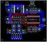
Alright, those are some very good suggestions, thanks for the help. By moving some of the resistors to the bottom of the board and moving the TDA and associated components closer I was able to shorten the paths a fair bit. Here is the picture.
Attachments
Gcollier said:
Alright, those are some very good suggestions, thanks for the help. By moving some of the resistors to the bottom of the board and moving the TDA and associated components closer I was able to shorten the paths a fair bit. Here is the picture.
Hi
Neat, good improvement.
In looking at this new PCB, I miss the decoupling caps close to both supply pins of the 8414, where are these located ?
- Status
- This old topic is closed. If you want to reopen this topic, contact a moderator using the "Report Post" button.
- Home
- Source & Line
- Digital Source
- Non OS TDA1543 PCB Layout