Hi Ken:
If I understand Hugsley explanation the idea is to fix Id (and fixing Id you fix Rd and voltage gain). To achieve that we need to evaluate Idss. The steps are:
- Obtain Idss and Vp (or Vgsoff) and select JFET with Idss between 200uA and 600uA (Id ~ Idss/3 to Idss/2).
- Id=100uA, then Rd = (Vdd/2) / Id (for a Vout = Vdd/2)
- From transfer curve or using equation Vp*(1-sqrt(Id/Idss)) (with 10% error) obtain Vgs.
- Finally Rs = - Vgs/Id
- Voltage gain is aproxx:
Av ~ 2 * (Idss / Vp) * (Vgs/Vp –1) * Rd
I think Rg=1Mohm is not necessary if you use magnetic pickup. A piezo pickup need Rg because (Hugsley please correct me if not) have more impedance (infinite resistance).
The idea of this preamp is to use between pickup and the rest of circuits (tone/vol/effects). Preamp act as impedance isolator (very high input impedance , low to medium output impedance)
The next circuit tells you if necessary a DC blocking output capacitor. For example, if go to amplifier directly, I think is not necessary (the amplifier have input capacitor).
Sorry for my english and I hope this helps.
Javier
Hi Javier,
Please pardon my ignorance but I do not know some terms.
I know :
Id is drain current,
Idss is drain current at saturation,
Vgs is voltage gate to source,
and I understand Vp or Vgsoff.
But what exactly is Vdd? Is it supply voltage?
Maybe you can help me calculate Rd and Rs.
I want Id = 100uA and Gain = 2.
My supply is 9 volts
Idss = 590uA
Vp = -0.82 volts
If you can tell me the values you calculate then maybe I can better understand the equations.
Thanks!
Ken
But what exactly is Vdd? Is it supply voltage?
Sorry Ken, yes, Vdd is supply voltage, 9V.
Maybe you can help me calculate Rd and Rs.
I want Id = 100uA and Gain = 2.
My supply is 9 volts
Idss = 590uA
Vp = -0.82 volts
The problem is that you can't fix gain because is a consecuence of fixing Id and the desire output operating point. Then I'll make step-by-step how to obtain Rd and Rs from Id and Vdd:
1_ Id = 100uA then Rd = (9V/2) / 100uA = 45Kohm
then Rd = 43kohm or 47kohm (more common)
2_ You can recalculate Id with the normalized Rd:
Id = (9V/2) / 47Kohm = 95.75uA
3_ Using transfer curve of your particular JFET (Id vs Vgs), obtain Vgs. I'll use the equation because I don't know your JFET. Then:
Vgs = -0.82V*(1-sqrt(95.75uA/590uA)) = -0.49V
4_ Rs = -Vgs/Id = 5114ohm. The normalized value is:
Rs = 5.1kohm
5_ Voltage gain:
Av = 2 * (Idss / Vp) * (Vgs/Vp –1) * Rd or
Av = 2 * sqrt(Id * Idss) / Vp
Av = 27
Is to much gain but I use JFET equations (with 10% error).
Av depends on Rd-Id (or Rd-Vgs), then we must reduce Rd or Id to reduce gain. But reducing Rd, Vout and Id increases.
Now, if you want to obtain Rd and Rs fixing Av and Id:
Rd = Av * Vp / (2 * sqrt(Id * Idss)) = 3376ohm
then Rd = 3.3kohm
Rs is calculated in the same way:
Rs = 5.1kohm
But now, Vout is Vdd-Id*Rd=8.67V!! (no swing for pickup signal).
Then, we can only fix 2 variables: Id-Av , Id-Vout , etc.
I think we must increase Vout (don't use Vdd/2) to decrease gain. But we must have room to signal and this depend on input signal level.
Well Ken, I'll wait JP Hugsley response to see what he has to say.
Javier
Hi Javier,
First, thank you for your help. You obviously have a better understanding of this than I. The equations you have shown here are what I was looking for, and your step by step explanation is Very helpful!
About the gain: I'm sure you are right. In his last post Mr. Hugsley used another resistor, from output to ground, to drop the gain from a figure of about 7 down to the level I needed - about 2. That's how the first JFET I saw lowered the gain (by Donald Tillman).
It's all academic anyway because I'm sure that the output resistor will not be used when the second stage of the preamp is integrated with the first.
As you say, we'll see what Mr. Hugsley has to say.
Thanks again,
Ken
Hi Ken:
Right! I forget the effect of output resistance (Ro) and the gain I calculated is with a bypass capacitor from source to ground.
The equations are (I used Avb for gain with bypass capacitor and Av without bypass capacitor):
With source capacitor:
Avb = (Rd//Ro) * 2 * sqrt(Id * Idss) / |Vp|
|Vp| means absolute value of Vp (0.82V in your FET)
Without source capacitor:
Av = 1 / [1/Avb + Rs/(Rd//Ro)]
In Hugsley circuit Ro >> Rd , so gain is little affected (may be will be more affected by the following stage).
Now, with Ro, you can adjust Av:
Ro = 1 / [(1/Av - 1/Avb)/Rs - 1/Rd]
So for your circuit (Rs=5100,Rd=47000,Av=2):
Ro = 14.5kohm
Correction from my previous post: you must use bypass capacitor at output if you want to adjust gain using Ro and input impendance from following stage.
Another thing I forget in my previous post:
Not only Idss is important, Vp too because will limitate voltage input. I don't know the level given by magnetic pickup but the max. input voltage peak to peak, Vippmax, will be |Vp| or less (|Vp| if Vg=0V at operating point). For your particular JFET, Vippmax ~ 0.8V. The "exact" value can be calculated using:
Vippmax = 2 * |Vgs - Vp|
I hope the circuit will be more clear to you with this explanation.
Javier
About the gain: I'm sure you are right. In his last post Mr. Hugsley used another resistor, from output to ground, to drop the gain from a figure of about 7 down to the level I needed - about 2. That's how the first JFET I saw lowered the gain (by Donald Tillman).
Right! I forget the effect of output resistance (Ro) and the gain I calculated is with a bypass capacitor from source to ground.
The equations are (I used Avb for gain with bypass capacitor and Av without bypass capacitor):
With source capacitor:
Avb = (Rd//Ro) * 2 * sqrt(Id * Idss) / |Vp|
|Vp| means absolute value of Vp (0.82V in your FET)
Without source capacitor:
Av = 1 / [1/Avb + Rs/(Rd//Ro)]
In Hugsley circuit Ro >> Rd , so gain is little affected (may be will be more affected by the following stage).
Now, with Ro, you can adjust Av:
Ro = 1 / [(1/Av - 1/Avb)/Rs - 1/Rd]
So for your circuit (Rs=5100,Rd=47000,Av=2):
Ro = 14.5kohm
Correction from my previous post: you must use bypass capacitor at output if you want to adjust gain using Ro and input impendance from following stage.
Another thing I forget in my previous post:
Not only Idss is important, Vp too because will limitate voltage input. I don't know the level given by magnetic pickup but the max. input voltage peak to peak, Vippmax, will be |Vp| or less (|Vp| if Vg=0V at operating point). For your particular JFET, Vippmax ~ 0.8V. The "exact" value can be calculated using:
Vippmax = 2 * |Vgs - Vp|
I hope the circuit will be more clear to you with this explanation.
Javier
JFET Biasing
Hi guys,
You both have posted some really good stuff but, I have to admit, I’m a little confused about the way you described the self-bias technique in your postings so I’m going to try and re-write the two self-bias techniques we have discussed so far (one using the square-law formula and the other using the graphic/experimental technique).
BTW: This is a long but straightforward explanation.
JFET self-bias “basics”.
Option-1: Bias a common-source amplifier using the square-law formula.
1. Evaluate the JFET to determine its unique IDSS and VGS-off values (in our case, we will use the J201 from my previous posting).
Once the Idss and VGS-off have been determined, and a Vgs point chosen (refer to Note 1), the “square law” formula can be applied to calculate a bias point for the JFET.
(Note 1: As a general rule-of-thumb, in order to maintain a good bias point for relatively linear operation, a Vgs point of between 1/3 to 1/2 your VGS-off value should be made.)
The “square law” formula is as follows:
Id = IDSS (1 – (Vgs/ VGS-off))**2
For the J201 I used for my amplifier in a previous posting, with an IDSS value of 0.51mA, a VGS-off of -0.77V (as shown in the diagram of the previous posting), and a Vgs = 1/2 VGS-off = -0.385V, the Id is calculated to be:
Id = (0.51mA) (1 – (0.385/0.770))**2 = 127uA
In order to achieve this bias point, a source resistance (Rs) of Vgs/Id is required:
For a bias point of 127uA and a Vgs of -0.385Vgs, the Rs would be 3.03 KOhm; the closest standard value being 3.0KOhm
(Note2: The square-law formula is an approximation for Id with results usually being within 10%, sometimes more.)
2. Now that we have a bias point and a value for Rs, the next thing to do is to calculate a Drain Resistance (Rd). Remember that the Id current through Rs is the same as through Rd and, with the rule-of-thumb that you want to have a Vd of between 1/2Vcc and 2/3 Vcc for linear operation, an Rd can be made by a simple application of Ohm’s Law.
For a Vd of 5.0Volts (between 1/2 and 2/3 that of a 9.0 Volt battery) you would have a value of 4.0 Volts across Rd (e.g. VD + VRD = 5V + 4V = 9V). To calculate the resistance of Rd, apply Ohm’s law:
Rd = 4.0Volt/127uA = 31 KOhm; the closest standard value being 30KOhm.
Choosing an Rg of 1.0MOhm, we now have all the values required to self-bias this particular common-source, J201 amplifier in the linear region.
Option 2: Self-bias a JFET amplifier using the “Graphical” or “Experimental” method.
Referring to a previous posting, and by using experimentally derived data-points and graphing (curve-fitting) software (e.g. Excel and Chart Wizard), it is possible to generate an accurate graph displaying the transfer characteristics of my J201 JFET.
The results achieved for Id and Vgs are very similar to Option 1 using the square-law formula but, in theory, this technique is slightly more accurate for the individual JFET being evaluated (and, potentially, more fun).
By observing the graph, a choice can be made on the locus that provides a near equal “swing” both above and below the bias point (again, this is usually found to be between 1/2 and 1/3 VGS-off). This method is quite subjective but nicely illustrates, graphically, the inherent non-linearities of the JFET. This is, in my humble opinion, part of what makes the JFET such an interesting device as a musical instrument amplifier (it is interesting to note that the locus of the graph is the inverse solution for any and all Rs values).
In the interest of battery-life, the bias point that I made was for an Id of 100uA which, according to my experimental data and not the square-law formula, corresponded to a Vgs of -0.38 Volts (about ½ that of VGS-off).
Once a bias point is chosen, the same techniques can be applied to calculate (using only Ohm’s law) Rs, Rd and Rg for proper operation:
Rs = 0.38 Volt/ 100uA = 3.8KOhm, the closest standard value being 3.9KOhm.
Rd = 4.0Volt/100uA = 40KOhm, the second closest value being 43 KOhm.
And an Rg of 1.0MOhm (this is considered to be a good input impedance for a guitar amplifier).
Conclusion: It can be see that there is a slight difference between the bias values chosen for the square-law formula technique and the experimental-data/graphical technique. The difference is most likely due to the approximate nature of the square-law technique and the subjective “rounding-off” and equipment calibration errors of the experimental technique.
Not-to-worry, they will both give you good linear operation for the particular JFET evaluated but, if I had to choose a technique for determining self-bias component values on a “onesy-twosey” common-source amplifier design, I would go with the experimental-data technique. If, on the other had, I was designing an amplifier for a production environment, I would choose another biasing technique entirely; one that would negate the individual and relatively “wide-spread” characteristics of the JFET (e.g. the Fixed-Bias technique).
Ken, let’s repeat this process using the “square-law” procedure for the values you experimentally derived using your J201 JFET:
Idss = 590uA
VGS-off = -0.82 Volts
Vgs = 1/2 VGS-off = -0.82 Volts/2 = -0.41Volts
Id = Idss(1 – (Vgs/VGS-off))**2 = (590uA)(1 – (.41/.82))**2 = 148uA
Note: 148uA is a good value for battery life; nearly 4,000 hours on a healthy 9Volt battery. You could, of course get more battery-life by using an Id of 100uA but this would affect the linearity of your particular J201. This may or may not be a problem. The J201 I used had slightly different IDSS and VGS-off values so the 100uA Id value was just about perfect in my design.
Using Ohm’s law: Rs = Vgs/Id = 0.41V/148uA = 2.7kOhm
For a Drain voltage of 6 Volts, you would have a voltage across Rd of 3 Volts.
Using Ohm’s law: Rd = VRd/Id = (3.0Volts)/(148uA) = 20KOhm
You could expect a gain of less than Rd/Rs = 20KOhm/2.7KOhm = 7.4
This gain could be lowered considerably by loading-it-down with a resistor after the Drain DC blocking cap.
Congratulations Ken, it looks like you did everything right!
Additional stuff:
Gain Factor: Javier, I really like the equations you've posted for calculating gain, I'm going to check-them-out with some real-world examples. However, it may be easier to calculate the gain of a common-source JFET amplifier intuitively by remembering that the current through the source resistor (Rs) is the same as the current through the drain resistor (Rd). Similarly, the change in current about Id (DC bias point) through Rs (produced by the vgs excitation voltage of a microphone or pickup) is the same as the change in current through Rd.
Hence, the gain factor of the common-source amplifier can be approximated via the ratio of Rd/Rs. This would be a gain factor or about 10 in my design with the actual measured gain factor being about 6.8. The measured gain factor will always be less than the ratio of Rd/Rs due to loading effects, local feedback and the non-ideal nature of the JFET as a transconductance amplifier.
Javier, I can tell you’re a fine mathematician.
Placement of the volume control: Javier, you are correct. For performance reasons, it is recommended that you always place the volume control after the preamp. The preamp should either be after the pickup or after the pickup selector switch (depending on how your guitar is wired).
DC Blocking Cap: Ken, you should place a DC blocking cap at the output of the JFET amplifier (at the junction of Rd and the drain terminal to either your tone circuitry or volume control). If you did not use a DC blocking cap at the output of your JFET, any resistances connected to the output of your JFET would completely change the DC bias point and, therefore, the performance of your amplifier. In addition, you should always prevent any DC voltages from occurring across your potentiometers (either volume or tone). If you do have DC voltage across your pots, you run the risk of audible “scratchiness” as you sweep the resistance value.
I hope this helps. Please let me know if you have any questions; if not, I'll go ahead and post the rest of the guitar preamp design.
JP Hugsley.
Hi Guys,
You are both excellent teachers; I've learned pretty much all I need to know (I think, lol). Your explanations are very clear and concise and I'm confident that they will work for optimizing pretty much any JFET amp stage.
The only question I have is about Mr. Hugsley's equation for obtaining Id:
Id = IDSS (1 ? (Vgs/ VGS-off))**2
Is the question mark after the 1 a square root symbol? Maybe it wouldn't translate to the forum here?
Other than that I'm ready to see the second stage.
You both have my thanks,
Ken
Hi Hugsley and Ken:
Hugsley, I think the confussion was because with option 1 (theoric) you start from Vgs=Vp/2 and with option 2 (experimental) you start fixing Id (making a balance between consumtion and linear operation). I started fixing Id directly (with both methods).
I checked some datasheets and I saw that the linear part of transfer characteristic is at 1/3*Vgs to 1/2*Vgs like you mention (and this Vgs values corresponds with Id values in the 2/3*Idss zone). But low Vgs implies high Id. I think we have to make a balance between desired Id value and selected Vgs point, taking into account the linear zone.
When using option 1:
Selecting Vgs = Vp/2, Id will be:
Id = Idss/4.
And if we want Vgs = Vp/3, Id will be:
Id = Idss * 4/9
Some points:
1_ I saw you use for Vd a Vdd*2/3 instead of Vdd/2. In this point there is no rule, right? This depends on output signal swing and gain?
2_ I agree with you about output bypass capacitor (OBC). I say to Ken that OBC is necessary if the following stage don't have a bypass cap.
3_ Gain:
Using your calculated values (and without Ro):
Avb = (Rd) * 2 * sqrt(Id * Idss) / |Vp| = 28.83
Av = 1 / [1/Avb + Rs/Rd] = 5.9
I derive gain equations from JFET equation and using the following definition:
Avb = (dId / dVgs) * Rd
And for your original circuit:
Avb = (Rd) * 2 * sqrt(Id * Idss) / |Vp| = 22.87
Av = 1 / [1/Avb + Rs/Rd] = 7.44
Obviously, these equations are not accurate because are derived from JFET equation and don't take account of Rds (dinamic resistance between Drain and Source).
Ken:
I saw correctly Mr Hugsley equations: is a minus.
Id = Idss * (1 - (Vgs/ VGS-off))**2
If you fix Vgs:
Id = Idss * (1 - (Vgs/Vgsoff))^2
And if you fix Id:
Vgs = Vgsoff*(1-sqrt(Id/Idss))
Both equations are equivalent.
Please Hugsley continue with following stage. After exams I'll post the idea I have to the new design (I want to transform TL082 based equalizer to JFET based).
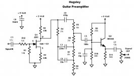
JFET Guitar Preamp
Hi Guys,
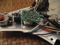
I have attached a schematic of the complete "on-board" guitar preamp. I will also try and post a picture of another on-board guitar preamplifier that I did about a year ago (the file may be too-big for DIY). Notice that the preamplifier circuit board is attached to the back of a standard Fender, 250KA potentiometer. This made for relatively easy mounting.
As you can see from the schematic, the guitar preamplifier is composed of three basic circuits: 1) The self-biased, J201, common-source amplifier, 2) A virtual copy of a standard Fender Bass and Treble tone control and, 3) The emitter-follower.
The J201 Amplifier.
We have gone over this aspect of the design in detail so there will be nothing mentioned about it here.
The Tone Control
This is essentially the Bass and Treble tone control of a Fender Deluxe Reverb guitar preamplifier. There is a slight difference in capacitor values due to impedance-scaling and the resistance values were chosen so as to emulate the Bass and Treble potentiometer "settings" that I prefer. The overall result is a slight Bass-boost (about 6.0dB) and a larger Treble-boost (about 10 dB) with the mid-frequencies (centered around 1KHz) "scooped-out" (by about 3 dB). These settings give the guitar a kind of "Bell-Chime" tone that really helps generate a "liveliness" to the overall sound. I realize these are subjective statements but you will just have to hear and judge for yourself.
The tone control topology used in this design is that of "attenuation" only; no "boost", only "cut". That is why you need gain in the first stage of your preamp; the tone control will cut the perceived gain of your J201 preamp stage significantly (a "cut" of nearly 12 dB overall).
By changing the resistance values in the tone circuit you can cut and boost a wide range of frequencies. You have the ability to "set" a tone that you like best. Then again, by adding a Bass and Treble potentiometer to your design, you can emulate the front-end of a Fender Deluxe Reverb right in the body of your guitar.
The Emitter-Follower
The Emitter-Follower is nothing more than a buffer that isolates the tone control and gain circuitry of the preamp from the un-predictable impedance of your guitar cable and guitar amplifier input. By using a 2N5088 transistor, you will get an affective output impedance of less than 200 Ohms. Other NPN devices can be used (e.g. the 2N3904 and 2N4401); these devices will have slightly less performance concerning input and output impedances but I doubt anyone could really tell the difference (maybe someone).
Conclusion
The battery-drain of this design is less than 180uA. That translates to a battery-life of more that 3,000 hours for a healthy 9 Volt battery.
I'm sure you will have some questions so please feel free to ask. I have had some pretty good results using this kind of topology for an on-board guitar preamplifier. I hope you do as well.
JP Hugsley
Hi Guys,
I have attached a schematic of the complete "on-board" guitar preamp. I will also try and post a picture of another on-board guitar preamplifier that I did about a year ago (the file may be too-big for DIY). Notice that the preamplifier circuit board is attached to the back of a standard Fender, 250KA potentiometer. This made for relatively easy mounting.
As you can see from the schematic, the guitar preamplifier is composed of three basic circuits: 1) The self-biased, J201, common-source amplifier, 2) A virtual copy of a standard Fender Bass and Treble tone control and, 3) The emitter-follower.
The J201 Amplifier.
We have gone over this aspect of the design in detail so there will be nothing mentioned about it here.
The Tone Control
This is essentially the Bass and Treble tone control of a Fender Deluxe Reverb guitar preamplifier. There is a slight difference in capacitor values due to impedance-scaling and the resistance values were chosen so as to emulate the Bass and Treble potentiometer "settings" that I prefer. The overall result is a slight Bass-boost (about 6.0dB) and a larger Treble-boost (about 10 dB) with the mid-frequencies (centered around 1KHz) "scooped-out" (by about 3 dB). These settings give the guitar a kind of "Bell-Chime" tone that really helps generate a "liveliness" to the overall sound. I realize these are subjective statements but you will just have to hear and judge for yourself.
The tone control topology used in this design is that of "attenuation" only; no "boost", only "cut". That is why you need gain in the first stage of your preamp; the tone control will cut the perceived gain of your J201 preamp stage significantly (a "cut" of nearly 12 dB overall).
By changing the resistance values in the tone circuit you can cut and boost a wide range of frequencies. You have the ability to "set" a tone that you like best. Then again, by adding a Bass and Treble potentiometer to your design, you can emulate the front-end of a Fender Deluxe Reverb right in the body of your guitar.
The Emitter-Follower
The Emitter-Follower is nothing more than a buffer that isolates the tone control and gain circuitry of the preamp from the un-predictable impedance of your guitar cable and guitar amplifier input. By using a 2N5088 transistor, you will get an affective output impedance of less than 200 Ohms. Other NPN devices can be used (e.g. the 2N3904 and 2N4401); these devices will have slightly less performance concerning input and output impedances but I doubt anyone could really tell the difference (maybe someone).
Conclusion
The battery-drain of this design is less than 180uA. That translates to a battery-life of more that 3,000 hours for a healthy 9 Volt battery.
I'm sure you will have some questions so please feel free to ask. I have had some pretty good results using this kind of topology for an on-board guitar preamplifier. I hope you do as well.
JP Hugsley
Attachments
JFET Guitar Preamp
The first picture file was too big. Attached is a "smaller" picture file of a similar JFET preamp I designed about a year ago. I mounted it in an American Standard Stratocaster.
Big sound from a little circuit.
Please let me know if you have any questions on how to adjust the tone or the gain of the Hugsley Guitar Preamplifier.
Thanks, JP Hugsley
Attachments
Alright! Now I can make one complete!
Yes, I'd like to adjust the tone. Is it simply a matter of trim pots? I know that would make it a little larger but I have plenty of room.
My Strat originally came with a preamp, but it was defective. I bought it anyway (got a big discount) knowing I could build one for it myself. What I had in mind at the time was an opamp design, but happily I have succumbed to the discreet component design and, well, here we are! So I have a cutout for the amp and even a battery slot in the back with its own cover - very accessible.
Great job, Mr. Hugsley! Thanks a Million!
And thank you, Javier, for your help as well!
Ken
JFET Guitar Preamp
Hi Ken,
If you do use trim pots for a versatile tone control, then try using two 100KOhm potentiometers (pots). The Treble control would take the place of R5 and R6 with the CW (or, top) terminal of the pot conected to C2, the wiper connected to C5 and the CCW (or, bottom) terminal connected to the junction of C3 and R7.
For Bass control, you must wire the pot as a "variable resistor" by soldering the wiper terminal to the CW terminal of the pot (so you end-up with a two terminal device) and use it to replace R7. With a pot value of zero Ohms you have full Bass-Cut, with a pot value of 100kOhm (full-CW) you have full Bass-Boost.
Like I said, the tone control is virtually that of a Fender Deluxe Reverb, only it has been scaled to use 100KOhm pots rather than the standard 250KA Ohm pots. You would have better control with audio-taper pots but linear tapers will work too (a bit "touchy" on the control though; e.g. the Bass-Boost will be near maximum with R7 at half value).
If you decide to just use resistors, remeber that:
With R5=0 Ohms and R6=100KOhms you have full Treble-Boost.
With R5=100KOhms and R6=0 Ohms you have full Treble-Cut.
With R7=100kOhms, you have full Bass-Boost.
With R7=0 Ohms, you have full Bass-Cut.
Ther is NO magic to the values that I have chosen so feel free to experiment with other values if you like.
More information: The 33p, C6 capacitor functions as a high-frequency roll-off cap. You can "cut" the high-frequency content of the preamp by making the value of C6 larger. Also, if you find that the signal level from your pickups is overdriving your JFET, you can increase the value of R12 to act as a voltage divider. In other words, if you make R12 equal to 470KOhm and R1 equal to 470KOhm you will cut the input signal level from your pickups by about 6dB (or, by "half").
Please let me know if you have any questions. Good Luck!
JP Hugsley.
JFET Guitar Preamp
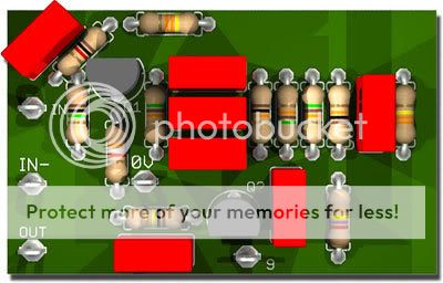
Hi Nico,
Wow, you work fast! That's great! I'm very happy that you found the design interesting enough to create a PC Board.
Thanks so much for giving me credit on the design. I hope you enjoy it and please let me know if you have any questions.
Take care,
JP Hugsley
Hi Nico,
Wow, you work fast! That's great! I'm very happy that you found the design interesting enough to create a PC Board.
Thanks so much for giving me credit on the design. I hope you enjoy it and please let me know if you have any questions.
Take care,
JP Hugsley
Do I need to make any major changes to use J309...? All I have at the moment...
At least the pinout is the same...
http://www.datasheetcatalog.org/datasheet/fairchild/J309.pdf
At least the pinout is the same...
http://www.datasheetcatalog.org/datasheet/fairchild/J309.pdf
JFET Guitar Preamp
Hi Nico,
Yes, there would be quite a difference in using a J309 instead of a J201 but it may still be worth experimenting with. The difference would be due to the fact that the IDSS of the J309 is between 12mA and 30mA, and VGS-off is between -1.0V and -4.0 Volt.
For arguments sake, lets say you "characterize" your J309, as described in my previous postings, and find that it is a middle-of-the-road device with an IDSS = 20mA and a VGS-off = -2.5V. Using the rule-of-thumb where Vgs = 1/2(VGS-off) = -1.25V and guessing that the Id would be 8.0mA (this is only a guess, you should verify all the specifications of your device as described in previous postings) you would then determine the resistor values to bias your common-source amplifier.
1. Rs = VGS/Id = (1.25V)/(8.0mA) = 157 Ohms or 150 Ohms
Using the rule-of-thumb that VRd = 1/3(Vcc) = 1/3(9.0V) = 3.0V;
2. Rd = (3.0V)/(8mA) = 375 Ohms or 390 Ohms.
Assuming that the values of IDSS and VGS-off are correct (these were only guesses) then the Rs and Rd values just calculated would bias-up your amplifier in the linear region for proper opearation.
However, there are two main differences that you would encounter:
1. The gain would be a little "low" for the Hugsley preamp. However, due to the realativley low output impeadance of your J309 amp as compared to the J201 amp, this may not be as big a problem as one would first think.
With a J309, you would get a gain factor of about 2. The J201 in the Hugsley preamp will give you a gain factor of about 6. However, due to the differences in output impeadances, you may still get a percieved signal that is reasonable (similar) at the output of the emitter-follower stage with the J309 (again, you would have to know the specifications of your J309 to calculate the difference).
Of course, you could always modify the EQ so that the attenuation is not so great but, in doing so, you may have to alter the "Fender Deluxe Reverb" topology a little (not really a problem). Experiment if you like, you may just like what you find better than the Hugsley values.
2. The battery-drain would be too high for practical use. With an Id of 8.0mA (The Hugsley preamp, with the J201, has an Id = 0.1uA) the battery would last no longer than 60 to 70 hours. This may not be a problem for you if you have easy access to your battery but it would not be very practical for a comercial product (it may end-up as the "number-one" customer complaint in your service department).
I would suggest that you evaluate your J309 as described in previous postings (for fun and practice) and then "solder-it-in" with with the proper biasing resistors.
Final pont: Although a fine JFET, there is nothing "magical" about the J201 or in how it is applied in the Hugsley circuit. Remeber that, as long as you qualify the differences and quantify the coresponding bias resistor values, you should have little or no problem in making this little preamp work with a variety of JFETs.
I would emphasize, however, that you must be aware of the trade-offs when dealing with various parameters like gain, battery-life, noise and transfer characteristcs in order to compensate effectively for optimal performance.
Keep me posted on how things turn out.
Good Luck, JP Hugsley
Very valuable, thread, I intend to go through it from the start with a calculator tommorrow...
I see that from a battery life point of view the original choice is much better... I had some J309 left from my rogic buffers, in which they sound unbeatable... Not such a big issue... I want to build it into my friend's guitar. He recently killed his pickups, got some new ones but did such a bad job wireing it up that none of the knobs work etc... I will build this plus a dynaComp compressor into the guitar...
The guy is realy good, just not rich... although he lately have been doing lead guitar for some commercial stuff and even a movie..
Hi guys,
Mr. Hugsley:
I wrote a program to calculate the various figures and values around the FET stage of your preamp using the "Square-Law" method. If I still had my O-Scope . . but I don't so I'll have to rely on this method.
Anyway, while I was writing the program a couple of questions came to mind.
1. In your example you set the Drain voltage to 5 volts but for my values you used a Drain voltage of 6. I know that both are within the 1/2 to 2/3 range recommended but, well wouldn't closer to the 1/2 mark be better to get an even swing, positive and negative, of the input? Is there a reason I'm missing for the varied Drain voltage and if so, how is it determined.
2. While I will build both stages of your design for my guitar, I have a friend who only wants the first, FET stage for his. I know that the gain for it needs to be "loaded down" to get within the range I want. On my test run I used the 10k you recommended and it worked fine. How can I determine the value I need to achieve a particular gain? Again, if I still had my Scope it would be easy to experiment and set.
Any light you could shed on either of these would be greatly appreciated.
Thanks,
Ken
JFET Guitar Preamp
Hi Ken,
There are essentially two reasons why I suggest the VD (Drain Voltage) of your JFET be biased between 1/2 and 2/3 your supply Voltage and both have to due with maintaining a symmetry in the output-voltage "swing" above and below your "bias point" (or, quiescent point):
1. The bias point will be "raised" by the value of Vgs (Vgs is equal to the Voltage "across" the source resistor (Rs)). In other words, if the Vgs (bias point) of your JFET is 1.0 Volt (Rs = 1.0V), then the mid-point between the voltage "across" the JFET (VDS) and the Voltage across your Drain resistor (VD) will be 5.0 Volts when a 9.0Volt supply is used.
Rs = 1.0V, VDS = 4.0V and VD = 4.0V for a total of 9.0V.
This would give you perfect symmetry of output voltage swing both above and below the bias point IF the JFET were perfectly linear (which, of course, it is not). However, as can be seen graphically in both the "Transfer Characteristic Curve" and the "VDS/ID Family of Curves" which are supplied in the JFET data sheet, the JFET is not perfectly linear.
This leads us to the second reason why I suggest you bias the JFET for a VD of between 1/2 and 2/3 the supply voltage.
2. You will notice in the "VDS/ID Family of Curves" that the spacings between the constant Vgs curves are not "equidistant". In other words, the difference (or, DELTA) in ID (Drain Current) will be greater as the Vgs moves incrementally from VGS-off (or, "pinch-off") to 0.0 Volts.
What this means is that there will be a non-symmetry about the bias point. The negative going voltage at the output of your JFET amplifier will swing more negative in value than it will swing postive in value (this can easily be seen on an oscilliscope with a "large-amplitude" signal just before "clipping"). For this reason, you will require a little more negative going voltage "headroom" with your amplifier than you will positive going "headroom" if you are to avoid un-equal "clipping" with large-signals.
What this all means is that, in order to acheive equal-headroom, you will need the bias point to be greater than 1/2 the supply voltage to compensate for both VRs (or, Vgs) and the non-linear voltage swing inherent in your JFET amplifier.
Although greater than 1/2 and less than 2/3 supply voltage is a good "rule-of-thumb" and will work well without verification, it really is best to verify your bias point with an oscilliscope as you suggest.
Concerning the "Square-Law" equation: by it's very nature, this equation is non-linear and, although used succesfully in the calculation of Id in a JFET, it must be remebered that it is only a simplified approximation that is usually within 10% of the real value.
On the bright-side of all this non-symmetry (or, non-linearity), this artifact is what gives rise to what is know as "even-harmonic-distortion".
Remeber that term because the manifistation of that particular non-linearity has been debated among audio enthusiasts as actually "enhacing the tone" of an amplifier (I hope I didn't open too big a can-of-worms with that last statement")
Concerning using just the first-stage of the preamp design; that's fine, experimenting with the design to best fit your application is what this exercise is all about.
To calculate how to lower your gain with a loading resistor is a straight-forward process using a variation of the voltage-divider formula.
Using the first stage of the Hugsley Preamp as an example, the output impedance is simply the Drain resistor value of 43 kOhm (although not exact, it is a good approximation) and, if you may recall, the gain of the first stage was about 6. If I want to lower the gain by half (or, to 3) then I would "load-it-down" with a 43 kOhm resistor after the AC coupling capacitor.
Other values can be calculated in the same manner using the voltage divider formula:
Vout/Vin = Gain = (RL/(RL + RD)).
Where RL is the load resistance and RD is the Drain resistance.
Remeber to only load the amplifier after the AC coupling capacitor.
I hope this helps,
JP Hugsley
Hi Ken,
There are essentially two reasons why I suggest the VD (Drain Voltage) of your JFET be biased between 1/2 and 2/3 your supply Voltage and both have to due with maintaining a symmetry in the output-voltage "swing" above and below your "bias point" (or, quiescent point):
1. The bias point will be "raised" by the value of Vgs (Vgs is equal to the Voltage "across" the source resistor (Rs)). In other words, if the Vgs (bias point) of your JFET is 1.0 Volt (Rs = 1.0V), then the mid-point between the voltage "across" the JFET (VDS) and the Voltage across your Drain resistor (VD) will be 5.0 Volts when a 9.0Volt supply is used.
Rs = 1.0V, VDS = 4.0V and VD = 4.0V for a total of 9.0V.
This would give you perfect symmetry of output voltage swing both above and below the bias point IF the JFET were perfectly linear (which, of course, it is not). However, as can be seen graphically in both the "Transfer Characteristic Curve" and the "VDS/ID Family of Curves" which are supplied in the JFET data sheet, the JFET is not perfectly linear.
This leads us to the second reason why I suggest you bias the JFET for a VD of between 1/2 and 2/3 the supply voltage.
2. You will notice in the "VDS/ID Family of Curves" that the spacings between the constant Vgs curves are not "equidistant". In other words, the difference (or, DELTA) in ID (Drain Current) will be greater as the Vgs moves incrementally from VGS-off (or, "pinch-off") to 0.0 Volts.
What this means is that there will be a non-symmetry about the bias point. The negative going voltage at the output of your JFET amplifier will swing more negative in value than it will swing postive in value (this can easily be seen on an oscilliscope with a "large-amplitude" signal just before "clipping"). For this reason, you will require a little more negative going voltage "headroom" with your amplifier than you will positive going "headroom" if you are to avoid un-equal "clipping" with large-signals.
What this all means is that, in order to acheive equal-headroom, you will need the bias point to be greater than 1/2 the supply voltage to compensate for both VRs (or, Vgs) and the non-linear voltage swing inherent in your JFET amplifier.
Although greater than 1/2 and less than 2/3 supply voltage is a good "rule-of-thumb" and will work well without verification, it really is best to verify your bias point with an oscilliscope as you suggest.
Concerning the "Square-Law" equation: by it's very nature, this equation is non-linear and, although used succesfully in the calculation of Id in a JFET, it must be remebered that it is only a simplified approximation that is usually within 10% of the real value.
On the bright-side of all this non-symmetry (or, non-linearity), this artifact is what gives rise to what is know as "even-harmonic-distortion".
Remeber that term because the manifistation of that particular non-linearity has been debated among audio enthusiasts as actually "enhacing the tone" of an amplifier (I hope I didn't open too big a can-of-worms with that last statement
Concerning using just the first-stage of the preamp design; that's fine, experimenting with the design to best fit your application is what this exercise is all about.
To calculate how to lower your gain with a loading resistor is a straight-forward process using a variation of the voltage-divider formula.
Using the first stage of the Hugsley Preamp as an example, the output impedance is simply the Drain resistor value of 43 kOhm (although not exact, it is a good approximation) and, if you may recall, the gain of the first stage was about 6. If I want to lower the gain by half (or, to 3) then I would "load-it-down" with a 43 kOhm resistor after the AC coupling capacitor.
Other values can be calculated in the same manner using the voltage divider formula:
Vout/Vin = Gain = (RL/(RL + RD)).
Where RL is the load resistance and RD is the Drain resistance.
Remeber to only load the amplifier after the AC coupling capacitor.
I hope this helps,
JP Hugsley
- Status
- This old topic is closed. If you want to reopen this topic, contact a moderator using the "Report Post" button.
- Home
- Live Sound
- Instruments and Amps
- New JFET guitar preamp project