JFET Guitar Preamp
Hello Javier and Marito,
Sorry it has taking me so long to post a buffer amp design but I had to think this one through. I decided to post a high-quality, discrete, two-stage buffer amplifier designed specifically as a 9.0V, low-current, on-board guitar preamp. I also decided to do this in two installments: the first on choosing and evaluating a JFET and the second as a description of the complete preamplifier.
I noticed that there are several postings about what JFET to use for the best "tone" and I'm sure everyone has their favorites but I decided to use a J201, N-channel JFET for the first stage of the preamp. This device was chosen mainly because it fit the criteria for the preamp design but also because I happened to have a couple laying about the shop.
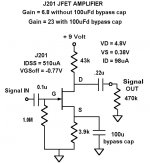
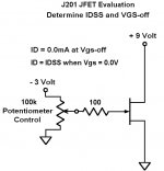
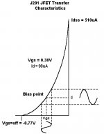
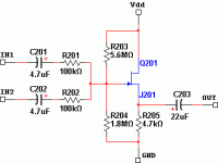
I have attached three (3) JPEGs: 1) The first shows an evaluation technique used to determine the Idss and Vgs-off of the J201 (JFET_Evaluation01), 2) the second shows the transfer characteristics of the specific J201 used in the design of the first stage of the preamp (JFET_Transfer01) and, 3) the last JPEG is a schematic of the first stage design of the preamp (JFET_Amp01).
It's a fairly straight forward process to determine the Idss and Vgs-off of a JFET and, if the topology of choice is a self-biased amplifier, it is highly recommended that such a process is applied due to the large variation in JFET characteristics; even within the same part type!
Manually determining the Idss and Vgs-off of every JFET would, of course, be a difficult thing to do in a manufacturing environment but, in the case of a "onesy-twosey" home project, it's not a problem.
I used a 9.0 volt battery as a power source and two 1.5 Volt batteries for the -3.0 V control-voltage. When the Gate and the Source of the JFET are "shorted" together and 9.0 volts is placed across the Drain and the Source you have, in essence, a constant current source; the current measured in this configuration is the Idss. In the case of the J201 I used, the Idss was 510uA.
By placing a negative voltage to the gate of the J201 with 9.0 Volts across the Drain and Source, I varied the negative control potentiometer until I had zero current through the JFET. This negative voltage applied across the Gate and Source was the Vgs-off; in the case of the J201 I used, the Vgs-off was -0.77 Volts.
These are good values for the buffer-preamplifier project because I wanted to design the first stage with a bias current of no more than 100uA and still be high-up enough the transfer cure to be linear with "small" signals.
In order to obtain an Id current of 100uA in the J201 using the self-bias JFET amplifier topology (very similar to the standard triode bias technique), I required a Vgs voltage of -0.38 Volts. To achieve this I placed a 3.9kOhm resistor from the Source terminal of the J201 to ground.
In order to have the Drain of the J201 biased at around mid power supply voltage (4.5V), I placed a 43.0 kOhm resistor from the 9.0V supply to the JFET Drain terminal. In addition, I placed a 1.0M Ohm resistor from the Gate terminal to ground to maintain a "high-impedance" at the input of the amplifier.
With the configuration shown in the Jpeg, I achieved a voltage gain of about 6.8 without the 100uFd by-pass capacitor across the Source resistance. In addition, I was able to achieve a voltage gain of about 23 with the 100uFd bypass capacitor across the Source resistor.
The question you are probably asking yourself is, "why do I need gain in a buffer amp'. The answer will become obvious in the next installment.
In the mean-time, please let me know if you have any questions about what I have posted so-far. I'll answer anything I can before we go on to the final design.
Thank you for your patience, JP Hugsley.
Hello Javier and Marito,
Sorry it has taking me so long to post a buffer amp design but I had to think this one through. I decided to post a high-quality, discrete, two-stage buffer amplifier designed specifically as a 9.0V, low-current, on-board guitar preamp. I also decided to do this in two installments: the first on choosing and evaluating a JFET and the second as a description of the complete preamplifier.
I noticed that there are several postings about what JFET to use for the best "tone" and I'm sure everyone has their favorites but I decided to use a J201, N-channel JFET for the first stage of the preamp. This device was chosen mainly because it fit the criteria for the preamp design but also because I happened to have a couple laying about the shop.
I have attached three (3) JPEGs: 1) The first shows an evaluation technique used to determine the Idss and Vgs-off of the J201 (JFET_Evaluation01), 2) the second shows the transfer characteristics of the specific J201 used in the design of the first stage of the preamp (JFET_Transfer01) and, 3) the last JPEG is a schematic of the first stage design of the preamp (JFET_Amp01).
It's a fairly straight forward process to determine the Idss and Vgs-off of a JFET and, if the topology of choice is a self-biased amplifier, it is highly recommended that such a process is applied due to the large variation in JFET characteristics; even within the same part type!
Manually determining the Idss and Vgs-off of every JFET would, of course, be a difficult thing to do in a manufacturing environment but, in the case of a "onesy-twosey" home project, it's not a problem.
I used a 9.0 volt battery as a power source and two 1.5 Volt batteries for the -3.0 V control-voltage. When the Gate and the Source of the JFET are "shorted" together and 9.0 volts is placed across the Drain and the Source you have, in essence, a constant current source; the current measured in this configuration is the Idss. In the case of the J201 I used, the Idss was 510uA.
By placing a negative voltage to the gate of the J201 with 9.0 Volts across the Drain and Source, I varied the negative control potentiometer until I had zero current through the JFET. This negative voltage applied across the Gate and Source was the Vgs-off; in the case of the J201 I used, the Vgs-off was -0.77 Volts.
These are good values for the buffer-preamplifier project because I wanted to design the first stage with a bias current of no more than 100uA and still be high-up enough the transfer cure to be linear with "small" signals.
In order to obtain an Id current of 100uA in the J201 using the self-bias JFET amplifier topology (very similar to the standard triode bias technique), I required a Vgs voltage of -0.38 Volts. To achieve this I placed a 3.9kOhm resistor from the Source terminal of the J201 to ground.
In order to have the Drain of the J201 biased at around mid power supply voltage (4.5V), I placed a 43.0 kOhm resistor from the 9.0V supply to the JFET Drain terminal. In addition, I placed a 1.0M Ohm resistor from the Gate terminal to ground to maintain a "high-impedance" at the input of the amplifier.
With the configuration shown in the Jpeg, I achieved a voltage gain of about 6.8 without the 100uFd by-pass capacitor across the Source resistance. In addition, I was able to achieve a voltage gain of about 23 with the 100uFd bypass capacitor across the Source resistor.
The question you are probably asking yourself is, "why do I need gain in a buffer amp'. The answer will become obvious in the next installment.
In the mean-time, please let me know if you have any questions about what I have posted so-far. I'll answer anything I can before we go on to the final design.
Thank you for your patience, JP Hugsley.
Attachments
as far as driving capacitive loads goes, the best way to drive into a high capacitance with unity gain buffers made with op amps is to use several (4 is convenient with a quad op amp such as a TL084) in parallel...
http://www.linear.com/pc/downloadDocument.do?id=25632
http://www.linear.com/pc/downloadDocument.do?id=25632
Re: JFET Guitar Preamp
Hi JP Hugley,
Just to add something to your explanation:
If you have different Vp and Idss values, you will need to use the following equations (if you didn't use this equations please correct me):
Vgsq = Vgs for operation point
Vgsoff = Vp = Vgs for Id=0
Idss = Id for Vgs=0
Igss = inverse saturation current (not considered in calculations)
Vp <= Vgsq <= 0V
Rs = -Vgsq / Idq
Vo = Vdd - Id*Rd => if we want Vo=Vdd/2 then
Rd = (Vdd/2) / Id
I have a few questions:
1-
Why do you choose Id = 100uA?
2-
Using FET equation (Vgs related to Id and viceversa):
Id = Idss * (1 - Vgs/Vp)^2 or
Vgs = Vp * (1 - sqrt(Id/Idss))
and with Vp=-0.77V, Id=100uA and Idss=510uA, I get:
Vgs=-0.43V, but you get -0.38V
3-
I calculate the minimum and maximum Vin using:
Vin min = Vp = -0.77V
Vin max = Idss * Rs = 1.989V
DVin = 2.76V
It's enough for piezoelectric pickups? I don't remember but I saw a signal from a piezoelectric pickup and it had a peak voltage of 3V (DVin=6V).
4-
With a gain of 6.8V and taking into account DVin=2.76V we have a variation in the output of DVo=18.77V (DVo must be below Vdd-(Vgsq-Vp)=9V-[-.38V-(-.77V)]=8.61V or 7.61V to have room for battery discharge).
Guitar Preamp
Hi Javier,
Yes, you are correct; what you have written is the equation quantifying the "square law" relationship between id and vgs. But you must realize that the equation is only an approximation that will agree usually to within 10% of the actual value of id based on Vgs-off, Idss, VDS and vgs. A more accurate equation for the transfer relationship of a JFET exits but it is based on the geometries, doping densities, doping gradients and voltage gradients of the JFET itself. If is much easier to use the "square law" equation but, better still, it is more accurate to determine the transfer relationship of your particular JFET experimentally for use as a "self-biasing" amplifier.
The exponent for the transfer relationship between id and vgs you used was "2" (hence, "square law") however, since the relationship is only an approximation, the exponent can actually vary between 1.5 and 2.5 for a more accurate fit. The "square-law" equation is only an approximation.
There are two reasons why I chose a bias current of 100uA. First of all, it is in a fairly linear region of the transfer curve derived experimentally for the J201 and, secondly, it allows a very low current drain from a nine volt battery (essential for an "on-board" guitar preamp). The gain of the J201 is a little less with a low ID value (proportional to the square-root of ID) but this is not a problem in our application.
Due to the fact that the "on-board" preamp in our discussion is being designed more for an electric guitar with an electo-magnetic pickup (not a piezoelectric pickup), gain is needed in the first stage. The "on-board" preamp is intended, specifically, for a Stratocaster, single-coil, electromagnetic pickup but can be modified for other applications. Of course, if the gain is too much for your application, you can always add a "pad" or attenuator to the first stage. But we can customize this later with real listening tests.
If you are worried about the gain being excessive for transients from the pickup you can "buy" yourself 6.0 dB of "headroom" by using two 9.0V batteries for an 18.0 Volt system but this may not be necessary. You may want to first conduct an A/B comparison test between a 9.0Volt and 18.0 Volt system. "Real World" evaluation and testing is essential in determining what best suits you're application.
Please let me know if this helps. Thanks, JP Hugsley
Re: Guitar Preamp
Hi JP Hugley:
Ok. Then the first step is to use a FET with Idss=200uA or more and follow these steps:
- Fix Id (Idq).
- With transfer characteristic obtain Vgsq
- Calculate Rs = -Vgsq / Idq
- DVin = function of Vgsq, Rs, Vp
- Calculate Rd = (Vdd/2) / Id for Vo = Vdd/2
- Voltage gain is: Av ~ 2 * (Idss / Vp) * (Vgsq/Vp –1) * Rd
Is this correct?
But, I have a piezoelectric pickup (PP) (the guitar actually have electromagnetic pickup, EP, but I added PP and thats why I need a buffer to mix the two signals). I don't touch the original circuit (EP, 9V battery, vol + tone controls): my idea is to mix both signals using this buffer. In both, I have the same signal level (2-3V peak).
Please, continue with the following part. Thanks.
Hi JP Hugley:
There are two reasons why I chose a bias current of 100uA. First of all, it is in a fairly linear region of the transfer curve derived experimentally for the J201 and, secondly, it allows a very low current drain from a nine volt battery (essential for an "on-board" guitar preamp). The gain of the J201 is a little less with a low ID value (proportional to the square-root of ID) but this is not a problem in our application.
Ok. Then the first step is to use a FET with Idss=200uA or more and follow these steps:
- Fix Id (Idq).
- With transfer characteristic obtain Vgsq
- Calculate Rs = -Vgsq / Idq
- DVin = function of Vgsq, Rs, Vp
- Calculate Rd = (Vdd/2) / Id for Vo = Vdd/2
- Voltage gain is: Av ~ 2 * (Idss / Vp) * (Vgsq/Vp –1) * Rd
Is this correct?
Due to the fact that the "on-board" preamp in our discussion is being designed more for an electric guitar with an electo-magnetic pickup (not a piezoelectric pickup), gain is needed in the first stage.
But, I have a piezoelectric pickup (PP) (the guitar actually have electromagnetic pickup, EP, but I added PP and thats why I need a buffer to mix the two signals). I don't touch the original circuit (EP, 9V battery, vol + tone controls): my idea is to mix both signals using this buffer. In both, I have the same signal level (2-3V peak).
Please, continue with the following part. Thanks.
JFET Preamp
Hi Javier,
I've been off-line for a week and I am just now getting back to DIY.
The calculations that you have written and your line-of-reasoning are correct. However, please understand that there are many JFET's available all with different characteristics. You must choose the one that you feel is best for your application. In my case, my primary concern is for "battery life"; for that reason, I decided on the J201 which can be biased between 50uA and 250uA depending on it's particular transfer characteristics. There are other JFETs that are optimized for noise and/or linearity but they may have much higher Idss and Vgs-off (pinch-off) values and, depending on the bias point, may drain a 9 Volt batter in less than 100 hours. With an overall current draw specification of 250uA for the entire on-board circuit, a nine volt battery can last over 2,000 hours.
For example, if you have a JFET with an Idss value of 3mA and a Vgs-off of -6.0 Volts, you may want to self-bias a common source amplifier with a Iq of 1mA. If you have two such amplifiers on your on-board circuit, that would be a total quiescent current draw of 2mA which would translate to a 9.0 Volt battery life of about 250 hours.
In any case, you would most likely bias your amplifier at about 1/3 the Idss value for best linerity (only a rule-of-thumb). For best results, you could, with a simple voltage source and current meter, determine the transfer characteristics of your particular JFET and, using Excel, graphically illustrate the transfer curve of any JFET you like (the accuracy would depend on the number of data points and the sophistication of your curve-fitting software).
The most striking realization you would have from such an excercise is discovering the large variation in JFET characteristics even among JFETs of the same part type.
Would you be interested in doing such an excercise? Would you like for me to send you some graphic samples of such an excercise?
Please let me know.
BTW: I have never designed a preamp for a piezoelectric pickup. It would help to know the source impeadance of such a pickup. Do you have this information? If not, could you give me the name and model of your guitar, maybe I could reseach this information myself.
Thanks, JP Hugsley.
Biasing
Hi guys,
First, I'm nowhere near you in the theory department but I have been building electronics for years and know a bit about it - enough to get me by.
But I'm having a problem biasing the Drain on this FET preamp circuit - not the one shown above, but Donald Tillman's:
http://www.till.com/articles/GuitarPreamp/
He recommends trying a few JFETs to get one with which the Drain bias will be 5 - 7 volts. I tried 10 of them and said bias is always 8.4 to 8.66 volts.
This bias is measured Drain to Ground, right?
I found this article:
http://www.diyguitarist.com/Guitars/FET-GuitarPreamp.htm
in which a trim pot is use for the 2.2k source resistor to make biasing easier. When I tried it the drain bias could indeed be set to around 6 volts and the circuit does work . . . Way TOO well. The amplification is far more than the 3.5 db described in the original article. I've seen the circuit used by lots of people successfully and I can't figure out why mine doesn't work. I've checked everything, even building two of them just to make sure I got it right.
I'm curious about how all the FETs I tried come out so similar and yet out of range.
Any ideas on why or how I can get this little beast in line?
I suppose I should just start over using the circuit shown above, but I don't like getting beat by such a simple device that everyone else seems to have no problem with.
Any info or pointers would be much appreciated.
Thanks,
Ken
JFET Biasing
Hi Ken,
The Fet circuit shown in Don Tillman's article is very similar to the circuit that I had written about in my previous postings. If you have not read my previous postings, this may be a good time to do so.
In any case, the amplifier is a self-biased, common-source design using the J201 JFET. The key term here is "self-bias", which simply means that the amp will bias up to a steady-state (or, quiescent) condition that is totally dependent on the devices "transfer characteristics" (again, this is explained in my previous postings).
In any class-A, linear amplifer (e.g. the Tillman design) you should bias the device so that the DC value at the output (in this case, the Drain) is equal to between 1/2 and 2/3rds that of the power supply (in this case, a nine-volt battery). This will ensure a relatively "equal" swing of an AC signal above and below the DC value at the Drain before "clipping" occurs.
When Tillman said that the DC value should be between 5 and 7 volts, he was referring to the voltage you would measure relative to the negative terminal (or "zero" volt reference) of the nine-Volt battery. This would mean that you have between 4 and 2 volts across the 6.8KOhm Drain resistor. According to Ohms law, this would also mean a bias current between 0.588mA and 0.294mA through the J201 (in the interest of conserving battery-life, I biased my amp to 0.1mA).
It is interesting to note that the J201 JFET I evaluated for the amplifier in my previous postings would not have worked well with Mr. Tillman's design. However, Tillman does say this when he mentioned that not just any J201 would work with the values he chose for his circuit. He suggests that you try a handful of them before you can find one that works well.
On the other hand, by evaluating the JFET and determining it's transfer characteristics (not a difficult thing to do as explained in my pervious postings) you can customize Mr Tillman's common-source, self-bias design for optimal performance (or, in other words, excellent symmetry about the Drain DC bias value).
Please let me know if this helps; if you have any questions, please do not hesitate to ask.
Thanks, JP Hugsley
First, thank you for your response!
Yes, I have read your previous postings on the subject though I didn't understand everything. I'm getting back into electronics after retiring from a career of programming so I need to brush up on terminology and theory. Also, much of this is new to me as most of my experience has been with opamps where my main considerations were gain and cutoff frequencies.
I think that perhaps I should consider using your schematic rather than Mr. Tillman's for a few reasons:
-It would conserve battery life a bit more.
-Am I correct in my impression that yours is not quite as picky about the particular JFET used?
-I like your gain figures better (6.8). And..
-I've exhausted all 10 of my transistors searching for one with the proper characteristics. There's no electronics store near me so I must wait for ordered parts.
I will try evaluating the FETs I have and study more carefully how to customize the circuit for proper performance
.
One question: If I use your circuit would the 10mfd decoupling cap across the battery still be a good idea?
You've been a great help and I really appreciate your time and effort.
Thanks again,
Ken
Mr. Hugsley,
After rereading your posts I realize now that the schematic you posted is the first stage of a guitar preamp. I thought it was the whole preamp due to its similarity to Donald Tillman's. Would it work without a second stage? What would be the advantages of a second stage?
Thanks,
Ken
After rereading your posts I realize now that the schematic you posted is the first stage of a guitar preamp. I thought it was the whole preamp due to its similarity to Donald Tillman's. Would it work without a second stage? What would be the advantages of a second stage?
Thanks,
Ken
JFET Bias
Hi Ken,
There is really no difference between the design that I posted and that of Mr. Tillman. They are both common-source JFET amplifiers; the difference is in the device itself. Even though they are both J201 devices, the variation in IDSS and VGSoff among J201 type JFETs is rather large. If you refer to a data sheet, you may be surprised to see that the IDSS for the J201 can be between 0.2mA and 1.0mA. In addition, the VGSoff can be between -0.3V and -1.5V.
From what I can tell, the device used in the Tillman design is on the high-side of the specification scale. In other words, the device he used most likely has an IDSS of 1.0mA and a VGSoff of -1.5V. The reason that I believe this is because he mentioned that the bias current in his circuit is about 0.5A. This means that the VGS is about 1.1V (0.5mA*2.2KOhm = 1.1 Volt) and the voltage drop across the Drain resistor (R3) is 3.4 Volts (0.5mA*6.8KOhm = 3.4Volts). This, of course, means that the Voltage at the drain of the J201 is 5.6 Volt (9Volt - 3.4 Volt = 5.6Volt).
(If any of this is not clear, please let me know and I'll explain it with a sheet of equations and diagrams).
The J201 device that I used in my circuit had a measured IDSS of 510uA and a VGSoff of -0.77Volts. If I had used my J201 in Mr. Tillman's design, it would not have worked very well (if at all). The bias conditions for my design were chosen to fit the particular J201 I had in my shop; this is what must be done when using the self-bias technique to ensure proper operation. From what you have told me, I believe the J201s that you have in your possession are probably more middle-of-the-road devices rather than the high-end-of-the-spectrum device Mr. Tillman used. In other words, there is nothing wrong with your JFETs, you just have to change the circuit values to best suit them.
Try changing the values of Mr. Tillman's design with one of your JFETs by making R3 = 20KOhm, R2 = 2.0KOhm and R4 = 10KOhm. R3 and R2 will give you a gain of nearly 7.0 (like my design) but R4 will load-it-down to a gain of about 2.0 (this is how you "tame the thing" as you called it).
In any case, don't throw away your JFETs, just evaluate them for IDSS and VGSoff as I described in my previous postings and then select component values to ensure optimal operation (biasing).
Again, if any of this in not clear, please let me know and I will make an effort to produce a paper that is more professional and concise.
Also, a 10uFd decoupling cap is a good idea to have on the circuit board as near to the active device(s) as possible. This will provide a zero-Ohm Voltage source for your circuit and help prevent issues with stray impedances.
Also again, the second-stage device on the design I was talking about in my postings will be an emitter-follower using a BJT. The advantage to an emitter follower stage is to isolate your active device and tone circuitry from the un-predictable loading effects of your guitar cable and guitar amp input impedance. This will become clearer in a future posting but, first, you should evaluate your JFETs and then optimize your common-source circuit design.
I hope this helps.
JP Hugsley.
Hi JP Hugsley:
Sorry for delay to answer (In this week I have 2 exams and I don't have much time).
The guitar is a Steinberger Synapse EMGSYN-GP-1. I don't have information about piezo. Check this page to see a picture.
In these days I'll make transfer curves using 5 or 6 2N3819 I have (In my city there are no J201 FET). I check a 2N3819 and obtain an Idss=1.3mA and Vp=-2.5V.
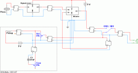
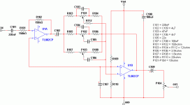
In these post and following I'll show my actual circuit. My idea is to replace equalizer with jfets (if possible) to reduce current consumption and the possibility to adjust circuit elements to achieve the best performance and low consumption.
Sorry for delay to answer (In this week I have 2 exams and I don't have much time).
The guitar is a Steinberger Synapse EMGSYN-GP-1. I don't have information about piezo. Check this page to see a picture.
In these days I'll make transfer curves using 5 or 6 2N3819 I have (In my city there are no J201 FET). I check a 2N3819 and obtain an Idss=1.3mA and Vp=-2.5V.
In these post and following I'll show my actual circuit. My idea is to replace equalizer with jfets (if possible) to reduce current consumption and the possibility to adjust circuit elements to achieve the best performance and low consumption.
Attachments
Hi Julian,
I need between 10 and 20 (I have to select the best for this circuit). My mail is xaviermdq arroba yahoo.com.ar.
Javier
I need between 10 and 20 (I have to select the best for this circuit). My mail is xaviermdq arroba yahoo.com.ar.
Javier
Andronico said:Hi, my name is Julián and live in Buenos Aires, how many J201 do you need ?
@ J. P. Hugsley
Hi,
I have evaluated my JFETs, writing their Idss and Vgsoff values on masking tape for future reference. I'm still not clear on how exactly to calculate the surrounding components for optimal results. I'd like to bias the amps at 0.1ma as you have to conserve batteries. I've read and reread your posts and though I have a much greater understanding of how the amp works, I guess I'm missing something. Can you point me to equations I can apply to calculate values for target currents and gain factors?
I'm happy to say that I built an amp following your recommended values as closely as I could: R3 = 21.5 k, R2 = 2.15k and R4 = 10k. This gave a voltage at the Drain of slightly over 6 volts. I know that's a little high but the amp does work so I tried it in my guitar. It's still slightly strong, overdriving the digital effects device I use unless the volume on the guitar is turned down to half or less, but usable. I noticed that when the guitar volume is turn down to 1 or 2 (out of 10) the high frequencies are being damped. Should I put the preamp between the pickup and the volume control? Also, should there be a DC blocking capacitor at the output?
Anyway it's working for now and I await your post of the second stage so I can build the complete preamp.
I really appreciate all your help and patience with one in unfamiliar territory. Instead of blindly following a schematic and a parts list with no explanation I am coming to understand how these work and learning to design my own.
Thank you very much,
Ken
- Status
- This old topic is closed. If you want to reopen this topic, contact a moderator using the "Report Post" button.
- Home
- Live Sound
- Instruments and Amps
- New JFET guitar preamp project