Yes, I have checked with the 10r waveform and there is a little difference in amplitude, 11Vpp in the high side instead of 12vpp in the low side. Don't think that's a problem. Can be due to the diode drop in the bootstrap circuit, right?
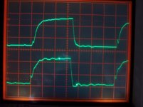
Please have a look at this: it is the 10r waveform. It shows a little more garbage in the turn-off phase, perhaps.
I will check with heavy load, however.
Best regards,
Pierrre
Please have a look at this: it is the 10r waveform. It shows a little more garbage in the turn-off phase, perhaps.
I will check with heavy load, however.
Best regards,
Pierrre
Attachments
Hi,
Yeah I believe that would be the cause of the difference, and I agree it isn't a big deal, I spotted a difference but couldnt' tell if it was 2 volts or....? No cause for concern there.
That gate step looks more pronounced in this screen, it's funny though I would expect to see that in the bottom driver. Let's see what happens with higher current")
Yeah I believe that would be the cause of the difference, and I agree it isn't a big deal, I spotted a difference but couldnt' tell if it was 2 volts or....? No cause for concern there.
That gate step looks more pronounced in this screen, it's funny though I would expect to see that in the bottom driver. Let's see what happens with higher current
That gate step looks more pronounced in this screen, it's funny though I would expect to see that in the bottom driver.
Sorry, don't understand you. What do you mean with "gate step", the little glitch that is attributed to the miller charge, or you mean the rise/fall times?. Why did you expect to see it in the bottom driver? (remember that the lower trace is HS driver in both screens).
Pierre
Well, yeah, the little glitch associated with miller.
I expected to see it on the bottom because it's the synchronous mosfet that's most susceptible to Cdv/dt induced turn on (it causes a "gate step").
I actually believe it can happen on the high side as well, but with good rail decoupling there it should be less of a concern.
Dead time and output current may play a roll here too. I'm curious to see what happens with more current flowing. Maybe you can check it at different output levels, low medium high? I suppose results will differ depending when you trigger it.
Don't rely on that captures more than necessary, perhaps the little gate step is there but the resolution of the oscilloscope has missed it in some of the drawings.
The "synchronous" mosfets is the lower one, right? That corresponds to the upper waveform in my captures. I think now I get you: in my waveforms the worse turn-off phase appears in the HS mosfet, that's not very logical.
Perhaps that's due to ringing instead of Cdv/dt, or simple parasitics in the oscilloscope lead (although I used 10x probe with a little tip with the grounding just by the tip to minimize the loop inductance that may pick up unwanted signals)
Yes, it will be hard to trigger. I think I will take a lot of captures for each power level to catch several duty-cycles and look for the unwanted spureous trials-to-turn-on.
I will also measure the PWM waveform looking for ringing or overshoot that could lead to avalanche.
Best regards
I expected to see it on the bottom because it's the synchronous mosfet that's most susceptible to Cdv/dt induced turn on (it causes a "gate step").
The "synchronous" mosfets is the lower one, right? That corresponds to the upper waveform in my captures. I think now I get you: in my waveforms the worse turn-off phase appears in the HS mosfet, that's not very logical.
Perhaps that's due to ringing instead of Cdv/dt, or simple parasitics in the oscilloscope lead (although I used 10x probe with a little tip with the grounding just by the tip to minimize the loop inductance that may pick up unwanted signals)
Yes, it will be hard to trigger. I think I will take a lot of captures for each power level to catch several duty-cycles and look for the unwanted spureous trials-to-turn-on.
I will also measure the PWM waveform looking for ringing or overshoot that could lead to avalanche.
Best regards
One thing more, about the coils, only to make sure they are not having influence on the failures.
I have tested the coil with a impedance analyzer. The results are:
-Inductance from about 500Hz to about 5MHz: 20uH.
-Resistance: about 30mOhm at DC, 180 mOhm at Fsw (270KHz)
-Capacitance: -16nF at Fsw.
saturation current must be quite high following micrometals inductance calculator (more than 20A).
The self-resonance is located at 10.6MHz. From there, the inductance is negative and the capacitance, positive.
What do you think of this?
Best regards,
Pierre.
I have done some measurements this morning.
About gates, they seem the same as what I have shown before, but it appears a nasty spike just before going up in both sides. This spike goes to about -5V. I don't know if it is a probe pickup, although I have measured it the same way as before. I am currently using FQP46N15's.
About the PWM waveform, it shows some undershoot of more than 20V amplitude in the negative side, and only with high power (tested with resistive load). I don't know if that's another noise pickup, but that makes Vds of the upper mosfet be about 120V. Perhaps more with another kinds of loads.
About VS pin with respect to COM pin, it doesn't show any apreciable undershoot, measure just at the IC pins.
What do you think about the coil measurements I have put in my previous post?
Seems that I am the only mad that works on weekend! ;-)
If you see my previous posts, you'll read that I have found some overshoot in the negative portion of the PWM signal increasing with higher power levels. That worries me and I was wondering whether reducing dead-time would help, as it would reduce the time that the signal is freewheeling...
Any opinions?
Best regards
Thanks, subwo1.
There are two undershoot problems, actually: the one in the gates (5V aprox), and in the PWM signal (more than 20V with high power output).
I don't know where the gates undershoot come from, perhaps it is only probe pickup.
But the other one makes me think that Vds(br) can be exceeded at some moment and cause mosfet failure. I also wonder why is it present only in the negative portion of the PWM and not in the positive.
Best regards
When you talk about a spike on the negative-part of the PWM - I assume that you mean a spike on the output signal when going low. This could be caused by the parasitic inductance of the FET (or any other circuit parasitic inductance as well of course), preventing the body-diode from turning on fast. I don't have an explanation why it doesn't happen on the positive-going side apart from differences in timing or maybe that it is indeed caused ba parasitics of the layout rather than the inductance intrinsic to the FET.
How does it behave whan you add a snubber ?
Regards
Charles
How does it behave whan you add a snubber ?
Regards
Charles
You're welcome. The gate voltage drop is caused by the Miller effect. It is not a problem at -5 volts. But the source undershoot could cause breakdown and avalanche and then smoke. Maybe try adding 1000pF from the totem pole outputs to ground to slow the transition some. The Miller effect will also be reduced, but hopefully enough will still remain to provide a little dead time.
Sounds good and you're welcome. In fact, go straight from the drain to the source of each MOSFET, I think, with a 470pF on each. If you can get away with 1000pF on each, it should be even better so long as there is still enough dead time. My experimentations with zero voltage switching leads me to believe this way.
If you can get away with 1000pF on each, it should be even better so long as there is still enough dead time
But how can the simple addition of the 470-1000pF between drain and source affect dead-time?
Zero voltage switching? I want to know, I want to know!

It should slow down the rate at which the voltage on the drains can flyback to the sources because of the output inductor. The result is improved switching too, so long as the inductor has enough stored energy to charge/discharge the capacitors during the transitions. By slowing down the transition, the Miller charging of the gate-source capacitance is kept from building as much because the series gate resistor shunts the charge as it is added. If the gate resistor is too small, and the d-s capacitors too large, the Miller effect will not be able to keep the gate unenhanced before the output finishes its transition. Then, the switching efficiency goes from the gain category to the loss side. It is a delicate balancing act to get it optimized.
The above mechanism is a type of adaptive dead time and is one element I am incorporating into my latest updated ZVS power supply. My ZVS power supply also needs phase feedback from the MOSFETs to the oscillator so that once the feedback shuts off each output switch, the opposite MOSFET turns on as soon as the voltage flies to its peak, which is ideally at the opposite power supply rail.
In classD, the phase feedback should not be necessary since the dead time is never capable of getting so high as it can in the ZVS power supply. In class D, when one MOSFET shuts off, the easiest thing is to let the output go straight to the other rail with no chance for extra dead time.
Adding "pure" capacitors can lead to increased overshoot. The snubber is actually representing a lossy cap which is 1.) reducing the Q of parasitic resonances and 2.) lowering the f0 of said resonances.
The 1nF cap with 1 to 100 Ohms (or your proposed 22 Ohms) in series is not a bad value to start with.
I would place it accross the Mosfet, since this is the component you want to protect with this measure.
Some may complain about the losses introduced by snubbers. These are not that severe however if you take enough care about a good layout with the subsequent need for very small snubbers only.
As long as the snubber's timeconstant is small enough that the capacitor is fully uncharged during each half-cycle the loss in the series resistor is calculated by (approx):
Ploss = C * 4 * Vpeak^2 * f
That means an amp running at 250 kHz and being capable of supplying 100 volts peak would actually produce 10 Watts of snubber loss when a snubber with 1 nF is being used. This might at first sound like being very much, but keep in mind that this very amp would drive a 4 Ohm load at 2500 Watts !
Regards
Charles
- Status
- This old topic is closed. If you want to reopen this topic, contact a moderator using the "Report Post" button.
- Home
- Amplifiers
- Class D
- Mosfet reliability in Class D amplifiers