
A series snubber with 1 nF and 22 Ohms in series has a time-constant of 22 ns which is not that much at all.
We must not forget that we do not just try to absorb a peak coming from some source (i.e. a parasitic resonant circuit that has been "triggered") we also try to influence said source by lowering its Q and resonant frequency, whereas the "Q part" is the really important one.
Regards
Charles
We must not forget that we do not just try to absorb a peak coming from some source (i.e. a parasitic resonant circuit that has been "triggered") we also try to influence said source by lowering its Q and resonant frequency, whereas the "Q part" is the really important one.
Regards
Charles
About adding a single capacitor across the mosfet, I have seen that as a experiment to determine the time constant of the resonant tank formed by the mosfet capacitance and stray inductance that is causing the ringing or overshoot.
But as snubber it is better IMHO to use a RC across each mosfet, as suggested.
One thing that I don't understand is why I don't get any overshoot at idle (no input) but it starts to appear as I increase the modulation. Isn't it due to the parasitics tank and hence independent on output current?
Best regards,
Pierre
PS: If you look backwards, I think that this thread is becoming a very useful and exhaustive reference that describes or at least proposes all problems that can cause reliability problems in class-D amplifiers. I hope it helps others too.
Please let me present a very complete reference on snubbers:
http://focus.ti.com/lit/an/slup100/slup100.pdf
Very exhaustive!
http://focus.ti.com/lit/an/slup100/slup100.pdf
Very exhaustive!
One thing that I don't understand is why I don't get any overshoot at idle (no input) but it starts to appear as I increase the modulation. Isn't it due to the parasitics tank and hence independent on output current?
This caused me thinking quite a lot
 OTOH this is what keeps our brains young (maybe) .
From a first glance I came to the same conclusion as you did. But the stored energy in the output inductor rises also with load current and therefore there is more around to "kick" some unwanted tank circuits. The fact that it is rising with load current would lead me to think that it could be the series inductance of the FET rather than a resonant circuit. OTOH it doesn't happen with the positive-going transient.

Regards
Charles
Perhaps the miller charge is acting to turn on the low side fet.
With increased output current, miller current would increase.
With too large a gate driver loop causing a springy source condition, that miller charge could bounce off the source inductance and slam back into the gate turning it fully on, while the other extra gate inductance from too large a loop would prevent the driver from reacting to it in time. This would occure I think as the high side fet turns off, inducing the dv/dt via miller to the gate, source/bounce back to gate.... POP, because it circumvents the dead time you're supposed to have, the driver no longer has full control over it at higher currents. That's my theory.
What else.. oh yeah, a -20V spike on the source, and a -5V spike on the gate, would seem to indicate +15Vgs and a fully turned on FET. So that seems to go well with the prior theory?
Regards
What else.. oh yeah, a -20V spike on the source, and a -5V spike on the gate, would seem to indicate +15Vgs and a fully turned on FET. So that seems to go well with the prior theory?
Well, in fact the -5V appears in Vgs voltages (not Vg). The fact that I see them in both high and low side makes me suspect that it is nouse pickup...
Pierre said:Well, in fact the -5V appears in Vgs voltages (not Vg). The fact that I see them in both high and low side makes me suspect that it is noise pickup...
Making noise free, high speed measurements is not trivial. You can check for common mode noise pick up by looking (measuring) at the exact point where you attach your 'scope probe ground lead (touch the probe tip to the end of the ground clip or whatever is in its jaws). Ideally you should see no signal - anything you do see is common mode noise that may mask the differential signals you really are trying to measure.
Reject this by running several turns of the 'scope probe cable through a large ferrite toroid (position it near the 'scope connector end). Also, you must use as short of ground lead as possible - preferably no ground lead at all. Special 'scope probe tip connectors are made for this purpose that allow you to remove the ground lead and tip cover (the witch's hat)
 and plug the bare probe right into your circuit board. These can be approximated with short lengths of wire soldered to your intended measurement point and nearby ground, and then wrapped curly cue fashion around the point and barrel of the bare probe. Leave them in place to receive the probe whenever you want to measure that signal again. (Some fuse clips seem to just fit the ground ring on the barrel of some probe tips and make nice connectors for that part.)
This may seem like a lot of trouble, but if you don't do it, you just may be going in circles chasing phantoms (IMO).
Regards -- analogspiceman
I completely agree with you, being sure of your measurements is crucial.
About the snubber, it is curious that I only have undershoot but no overshoot in the positive portion of the PWM signal. I currently don't have a sense resistor that could cause too much inductance in the source path, but let's see...
I have simulated a snubber and taken the opportunity to include the current sense circuit based on Rds(on) that subwo1 proposed. It seems to need a few pF at the output (perhaps the SD pin or wherever it goes capacitance is enough) to filter the recovery peak, that is higher than the voltage to measure.
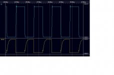
Upper trace is Vds (a single mosfet has been simulated, a IRF640 with 50nH series inductance and a 470pF+10ohm snubber).
Lower trace is output of the current detector circuit.
About the snubber, it is curious that I only have undershoot but no overshoot in the positive portion of the PWM signal. I currently don't have a sense resistor that could cause too much inductance in the source path, but let's see...
I have simulated a snubber and taken the opportunity to include the current sense circuit based on Rds(on) that subwo1 proposed. It seems to need a few pF at the output (perhaps the SD pin or wherever it goes capacitance is enough) to filter the recovery peak, that is higher than the voltage to measure.
Upper trace is Vds (a single mosfet has been simulated, a IRF640 with 50nH series inductance and a 470pF+10ohm snubber).
Lower trace is output of the current detector circuit.
Attachments
OK I've been doing brushing up on some old reading.....
Why it's worse with increased output current/non existant with low current :
dV/dt = I/C
Where C is the total node capacitance, ie: parasitics, snubbers, etc.
So, >I=>dV/dt = body diode problems=..... parasitic BJT turn on??
So, a snubber should help by increasing the node capacitance thereby slowing dv/dt.
A larger gate resistor may help by slowing down dv/dt but while not an optimal method may be interesting to try anyway, though it would still be dependant on output current..... not a good fix at all.
A larger inductor to keep current lower will also decrease dv/dt.
Perhaps the best compromise all around in this case would be to add a suitable shottky parallel to the body diode to ensure the body diode doth not conduct, then you can keep your high current, and your fast switching, and your lower thd.
Them's yer options as I see them.
Pierre said:I have simulated a snubber and taken the opportunity to include the current sense circuit based on Rds(on) that subwo1 proposed. It seems to need a few pF at the output (perhaps the SD pin or wherever it goes capacitance is enough) to filter the recovery peak, that is higher than the voltage to measure.
Hi Pierre, it is a good idea to add the little extra capacitance. I usually get by without it in the simulations so long as you remember that many logic gate models omit the built-in 5pF capacitance, but add some in real circuits sometimes as a precaution. But it helps to connect the diode from the lower gate driver output before the gate resistor to pull or hold the SD gate low as soon as possible. I have tried other protection methods, but I think this one is my favorite and the best performing for the simplicity.
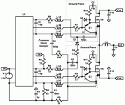
If I were building a DIY class D amp for myself, I would put the driver circuitry on little daughter boards above the main PCB in order to solve the routing conflict around the output mosfets between power and drive signals. I would contact the mosfet leads using traces to the edge of the little board at about 5mm below the body of the mosfets and fix the connections with solder from just the front side of the mosfets. One side of each of these boards would be a solid plane connected to the source of its mosfet. The signal leads to the driver IC (which would be on the main PCB) would each be a twisted triple of kynar wire routed through an approximately 5mm diameter by 10mm long ferrite bead. This would decouple the driver IC from the mosfet switching edges and ringing on both the high side and the low (ground) sides. Please see attached schematic.
Regards -- analogspiceman
Regards -- analogspiceman
Attachments
Some considerations: I am taken for granted that the diodes I am using for the gates and for the VS to COM protection as well as for bootstrap are adequate: they are MURS120. They are ultrafast, not schottky.
Here is the datasheet:
http://www.onsemi.com/pub/Collateral/MURS120T3-D.PDF
Do you think that there can be any problem with them?
Particullarly the VS to COM diode: it is effectively in parallel with the lower mosfet, it was intended to protect VS pin from going too negative. Perhaps this needs a review now.
Best regards
- Status
- This old topic is closed. If you want to reopen this topic, contact a moderator using the "Report Post" button.
- Home
- Amplifiers
- Class D
- Mosfet reliability in Class D amplifiers