subwo1: excellent, that circuit is simple enough to worth a deeper view.
I suppose that circuit uses Rds(on) to sense current. I understand the need for a latching for this application. Modifying that by using a latch should not be difficult.
However, I see some drawbacks (take them as suggestions only")
Rds(on) is dependent on temperature, so sensitivity or overcurrent trip level will also be. That's not bad per-se, as current limit will be lower as temperature rises, so it is very safe.
Best regards
I suppose that circuit uses Rds(on) to sense current. I understand the need for a latching for this application. Modifying that by using a latch should not be difficult.
However, I see some drawbacks (take them as suggestions only
Rds(on) is dependent on temperature, so sensitivity or overcurrent trip level will also be. That's not bad per-se, as current limit will be lower as temperature rises, so it is very safe.
Best regards
They only seem to say that the driver tolerates the difference.. further investigation on that would be nice, but for a quick n simple way, would it be alright to short the Vss and Vcom pins together? If so that might be telling enough.
Connecting those pins together is the most ordinary way to use this IC but a part of "most ordinary" means also usage without sense resistor.
I have to search again for the info about the negative supply voltage difference. On the IR2110 datasheet you can see that they recommend not to go beyond +- 5 Volts while they can bear quite some more actually (max ratings section).
Regards
Charles
Thanks, Pierre. Indeed, as the MOSFET heats, a trigger would trip sooner. Since a 74C14 contains 6 gated outputs, the output of the triggered gate could pass to another input whose output is fed back to to the first gate through a diode to latch it.
For 45v rails, the rectifier diode could be traded in for a 1n4148 so that junction capacitance can be minimized, improving performance. In one power supply circuit, I replaced that UF4004 with a series of 1N4148 diodes which did two things. It increased the breakdown voltage and in the other direction the forward voltage drop was the determining factor for when the protection would kick in.
For 45v rails, the rectifier diode could be traded in for a 1n4148 so that junction capacitance can be minimized, improving performance. In one power supply circuit, I replaced that UF4004 with a series of 1N4148 diodes which did two things. It increased the breakdown voltage and in the other direction the forward voltage drop was the determining factor for when the protection would kick in.
No problem, when the lower MOSFET is on, the LO is high so that a rising ds voltage on that MOSFET lets the resistor connected to the gate pull the shut down pin up to trigger it. The instant LO goes low, the diode connected to it quickly pulls down the sd pin prevent interference with the next half cycle of the waveform output.
It's very much OK, good perception about low Rds-on MOSFETs, too. Let's see. If Rds is .025R, and the current is 20a, we get half a volt to trigger within. I think it is doable. It triggers instantly, but since the speaker is DC coupled to the output, if we just truncate the lower on-time, we could get a heavy DC Bias on the output. I wonder if the feedback circuit of the amp will cut off the upper MOSFET in order to try to re-establish balance. But if we figure that the amp is the problem in the first place, we need to latch a separate external trigger which can use diodes to pull down both inputs to the IR2110 and hold them low.
I assume that you worry about that DC problem with the circuit "as it is". I agree, but as soon as you put a quick reacting latch, it will proctect well.
If I understand well, focusing on the half-cycle where LS mosfet is ON: you have a voltage divider from 12V (LO output) to VSS+IxRdson plus a diode drop. So if there is no loading,
you have 0.7V+ 11.3*30k/(82k+30k)=3.9V aprox.
If you have, say, 20A and a Rds(on) of 60mohms, you have about 1.2V+0.7V+(12-1.2-0.7*30k/(82k+30k))=4.6V aprox.
Am I calculating ok? I suppose that the trimmer way is how one finally does this.
Doesn't seem quite right. Lets break it up into bits, especially since I am not good with math. The first part is good, the voltage floor is the 1.2v drop across the MOSFET plus the .7v diode drop--1.9v. The LO pin is at 12v, OK. The trigger point is about 1/2Vcc + 1v, or 7v, maybe 7.5v really. 12v-1.9v=10.1v; lets round to 10v. Now we figure the voltage divider. 30k+82k=112k. 112k / 10v = 11.2k per volt, rounded to 10k/v. 30k / 10k/v= 3v. 3v plus the 1.9v floor equals 4.9. Good job! You had it right with the single formula. How, I don't know.
So as it is it trips at about 20amps. Trying to get it exact this way can lead to brain damage. Using a trimmer pot is an easier way. Best to place in the lower leg of the divider so that if the wiper contact opens up, the trigger point will drop. However, just using a two resistor divider does eliminate that concern.
So as it is it trips at about 20amps. Trying to get it exact this way can lead to brain damage. Using a trimmer pot is an easier way. Best to place in the lower leg of the divider so that if the wiper contact opens up, the trigger point will drop. However, just using a two resistor divider does eliminate that concern.
Hi,
I can also wholeheartedly reccomend subwo's desaturation protection circuit. I use similar circuit (only instead triggering SD pin i trigger small SCR that discharges driver supply caps and demands manual restart). I did not have a single dead Mosfet in 3kW PFC design over last 5 years.
Charles,
thanks for taking your time and drawing a nice illustration of proper way of minimizing loop inductance. I think that people grossly underestimate importance of tight loops in layout. A most common thing I see is bypassing electrolytics with film caps. Encouraged by Guido Tent's comments (and Bruno's) I recently measured a lot of different electrolytics and other caps on HP impedance meter that can go up to 13 MHz. All wound foil film caps have higher inductance than electrolytics. Stacked foil caps are comparable. The most shocking was smal no name 1uF/50V electrolytic i pulled out of dead ATX power supply. It measured 3nH, the same as 2-3mm diameter loop of wire. For comparison, Oscons have 6 to 9nH of inductance and 1cm square loop of wire has 17nH. So what is the point of bypassing 12nH electrolytic with structure that can easily have 30-40nH of inductance, small C and low ESR. It only makes things prone to ringing.
But there is a little trick that TI uses in their class Damps. They use around 100nH inductor (IIRC) in positive rail and then series RC snubber directly across supply pins of Mosfet totem pole. I think that there is even patent for that, that dates back in Toccata times (before TI bought them). Hopefully I will find it again.
Best regards,
Jaka Racman
Even more! I wondered about the stable threshold when i've studied ir2127.pdf. The diode placing close to the mosfet(for the equal temperature) lend pretty stable current threshold. IRF3205@50A@+1N4148@9mA =.989V100C° and 1.083V20C°.Rds(on) is dependent on temperature, so sensitivity or overcurrent trip level will also be. That's not bad per-se, as current limit will be lower as temperature rises, so it is very safe.
Do any of the diodes need to be schottky or can it be implemented with two 1n4148?
I am thinking on doing an experiment, but using a lower trigger point, say 1V, to excite a transistor that latchs, etc.
BTW: I removed the damaged mosfets from my last amp. They _were_ NTP35N15. One of them has three pins shorted together, the other one doesn't have a short in the gate to the other pins (only between S and D). I suppose this doesn't tell anything about the failure mode...
The failed amp didn't have the sense resistor, either, only a thick tin short. So that doesn't seem to be related either.
Best regards
Hi Pierre,
I use MUR106 for offline applications. I suggest you use a low reverse capacitance diode like 1N4148. Schottkys have large capacitance and even worse: significant leakage current.
I think that for Mosfet protection triplevel is not very important. Something else is if you want exact current limiting. I think that with desaturation protection you can forget about exact current limiting and use thermal protection instead.
Best regards,
Jaka Racman
After reviewing a bit more the Cdv/dt issue, some of the app notes talk about watching at the gate waveform to see the spikes that can cause spurious turn-on if they reach Vth.
I have a question here: this problem doesn't seem to have nothing to do with drain currents, so it should manifest even at light loads. I mean, if that's the problem, a spike should be seen when the Vgs voltage is low and the other mosfets is turning on, right?
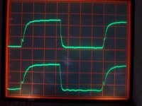
I checked my gate waveforms with both 6 ohm and 10 ohm gate resistors, with load but no input signal, and they looked this way. I attach the 6 ohms one, the other is almost identical, a bit slower. Can I stop worrying about Cdv/dt then?
The little spike at turn on should be due to the miller charge, but there are no spikes when the mosfet is turn off...
I have a question here: this problem doesn't seem to have nothing to do with drain currents, so it should manifest even at light loads. I mean, if that's the problem, a spike should be seen when the Vgs voltage is low and the other mosfets is turning on, right?
I checked my gate waveforms with both 6 ohm and 10 ohm gate resistors, with load but no input signal, and they looked this way. I attach the 6 ohms one, the other is almost identical, a bit slower. Can I stop worrying about Cdv/dt then?
The little spike at turn on should be due to the miller charge, but there are no spikes when the mosfet is turn off...
Attachments
Hi,
It looks like there's a bit of a step on the lower one. What's that at 5V/div? ~.5V gate step with no substantial output current, why not give it a try with output current and compare them, it just may get worse.
Hey, are those on the same scale? How do they measure pk-pk it almost looks like they aren't the same.
Hi, I think the bigger problem may actually occur when the lower gate is being pulled low, but the Miller effect occurring when the upper MOSFET is pulling its drain high is trying to turn it back on. It may be showing up in the thickened portion of the falling edge of the gate waveform and appears to happen within a very short time interval.
Hi Jaka, we practically crossed in our postings, but I am glad that we said practically the same thing concering the 1N4148 diodes.
Hi Jaka, we practically crossed in our postings, but I am glad that we said practically the same thing concering the 1N4148 diodes.
Thanks for the soon response to both of you. I love this forum and how helpful people is in it.
The lower one is actually HS mosfet. Yes, the scales are the same. It seems that the HS has a little less amplitude. I will check the other figure (with 10 ohms) to see if it happens the same.
Have in mind that both waveforms are not taken at the same time, so time is not aligned.
I will check with heavier load (I will need to trigger with a digital storage oscilloscope, as the signal moves its duty cycle when a large signal is present).
Best regards,
Pierre
- Status
- This old topic is closed. If you want to reopen this topic, contact a moderator using the "Report Post" button.
- Home
- Amplifiers
- Class D
- Mosfet reliability in Class D amplifiers