Yes, you are right.
I reviewed the calculations after posting and found that results are not so good: using eq. 12, you have:
For IRF640N:
Qgs/Qgs1=300pF*(100-4)/(1200pF*4)=6 !!!
How can this work reliably in earlier ZAP Pulse modules, then?
Another thing that I don't understand is that this equation doesn't show relationship with dV/dt, so having this high ratio musn't make us discard that mosfet for 100V operation, right?
Yeah that's disgusting isn't it?
Now that doesn't account for the heating caused by it, the level of current that will flow, or for that matter if it will turn on so hard that it explodes. All that tells is that it isn't an optimal device to use for the synchronous mosfet, because it will no doubt be heating like crazy as the gate step is more than big enough to cause substantial current flow in this case.
When I used them they both ran hot as hell but the circuit wasn't "right" so I can't attest to that really, also it was much lower voltage.
You know what though, you should do that calc with Vth min, that's basically when current flows, which is 2 volts, which doubles your answer to ~12. Ewwwww.
Now try it again with this puppy using Vth min of 2volts:
http://www.fairchildsemi.com/ds/FD/FDP42AN15A0.pdf
I wasn't very uptight about selecting the capacitance values,
I used Crss=20pF and Cg~2nF, and it's actually probably higher than 2nF.
I got ~ 0.45! How is that for a leap in technology?
Hey,
To make things more complex. Look at the graphs showing the caps vs voltage.
You will find that at low voltages the caps are higher, at least some.
And yes, adding Cgs externally can't cure what is going on inside
the transistor case but may still help a bit from the drivepath point
of view. The cap must be as close to the transistor pins as possible.
Also, all drivers and FETs leak current so adding a 10k resistor at gate-source is nice.
/ Mattias
Hi Mattias,
We actually are reading the cap values off the graph in order to account for the changing capacitance with voltage. Miller capacitance is hugely non linear.
You can't use the given capacitance values found under the max values (?) section for the same reason you just can't use the given charge ratio's ..... even when it seems like they are giving you the relevant charge ratio's, the reason is because those values were taking at what is likely to be different conditions than you're interested in.
An interesting point about this is due to the changing capacitance Vs voltage, you might find a mosfet that gives an OK ratio for one particular voltage but not for another.
As far as selecting mosfets, I think the pro's are privy to some information we may not be as well, like if you're going to be ordering 10 000+ you can talk to sales reps or maybe even designers and perhaps get some recommendations etc.
Fairchild devices seem to be pretty good with their charge ratio's, I have yet to check any of IR's decent mosfets for it.
Note that the IRF640 they were done for here was the old version and not the IRF640N, it maybe interesting to do them both.
You'll still find app notes that show this method isn't accurate but I believe it is OK for a ballpark idea which is all we're really after here anyway.
.....mosfets...... and they said they were easy to drive.
And yes, adding Cgs externally can't cure what is going on inside......
To make matters worse, the lead inductance will give some more uncertainty on what's going on inside and what we see outside.
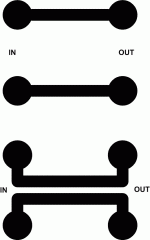
That's also the thing I'd like to mention regarding Pierre's layout. It is not only the LENGTH of the tracks in the gate-drive circuit that are critical but also the SHAPE. The loop inductance is very important. Have a look at the following drawing. The second loop has less inductance than the first one despite the longer track lengths.
Regards
Charles
Attachments
Sorry, I made a mistake with IRF640N.
The ratio should be something near 1-1.5 (at Vds=100V)
And for IRF640, it is about the same.
BTW: classd4sure, I think ZAP pulse used IRF640N, not IRF640, look at the photos in their webpage ;-) Anyway, they are similar in this particular aspect.
Curious: my FQP46N15 seems to have a ratio of about 0.5 at 100V. However it failed once (although in the lab, perhaps I did some short-circuit :-(
NTP35N15 is difficult to calculate por 100V, but seems to have a ratio higher than 1. It has failed in my circuit several times.
Best regards
Pierre I believe I made the same mistake as you, voltage we used to read the cap value was 10V wasn't it, I suppose it would make some difference ")
I cooked two sets of FQP46N15's myself, making the point everything needs to be perfect. You've just taken measures to be less concerned that they could be frying from a Cdv/dt induced spurrious turn on issue, however, that seems to imply an ideal layout and everything.
Let's say you have a "springy" source issue, due to layout, the Cdv/dt immunity might make it a bit more rugged and so it may last longer but it doesn't mean it can't fail from it. Maybe this is what you're experiencing.
Charles,
All I knew about "shapes" was "no sharp turns" and I understand why, in this case I would like to understand more, what is the mechanism at work to cause the second loop to have less inductance?
Thanks
I cooked two sets of FQP46N15's myself, making the point everything needs to be perfect. You've just taken measures to be less concerned that they could be frying from a Cdv/dt induced spurrious turn on issue, however, that seems to imply an ideal layout and everything.
Let's say you have a "springy" source issue, due to layout, the Cdv/dt immunity might make it a bit more rugged and so it may last longer but it doesn't mean it can't fail from it. Maybe this is what you're experiencing.
Charles,
The loop inductance is very important. Have a look at the following drawing. The second loop has less inductance than the first one despite the longer track lengths.
All I knew about "shapes" was "no sharp turns" and I understand why, in this case I would like to understand more, what is the mechanism at work to cause the second loop to have less inductance?
Thanks
Pierre I believe I made the same mistake as you, voltage we used to read the cap value was 10V wasn't it, I suppose it would make some difference
Yes, 10^1=10, not 100!!!!

I cooked two sets of FQP46N15's myself, making the point everything needs to be perfect. You've just taken measures to be less concerned that they could be frying from a Cdv/dt induced spurrious turn on issue, however, that seems to imply an ideal layout and everything.
Yes. I have also thought on adding a gs resistor (1-10k). And a zener in antiparallel with Vgs to limit the max. Vgs to about 15-18V. Just to protect the gate.
About the "springy" source, I suppose you mean the high side mosfet source, going below -vcc, right? I suppose I have to measure that properly too in the lab.
BTW: IRF ref. design uses IRFB23N15 that has a ratio of about 1.5 at 100V. They also seem to be reliable and they don't use anything sophisticated in the gate drive, just IR2xxx + 9.1R gate resistor + antiparallel schottky. Mmmmm.
Charles, I would also like you to enlighten us a bit more about reduction of inductance in the tracks!
Best regards,
Pierre
Simply because the loop is basically an (air cored) inductor with only one turn.
If you now look at the literature you will see that a coil's inductance is proportional to its AREA, the square of its number of turns and the inverse of its length (which is almost zero in our case). The enclosed area of the second loop is clearly smaller than the first one's.
There is a Tripath Appnote that describes these things quite well and you see it also mentioned on some IRF docu. I don't know how reliable Tripath's demo boards are but they seem to get away with quite long tracks between the driver and the output FETs.
We may never forget that it is sometimes only small details that make the difference between a reliable and an unreliable design.
Regards
Charles
About the "springy" source, I suppose you mean the high side mosfet source, going below -vcc, right? I suppose I have to measure that properly too in the lab.
I mean say you have too much inductance in the driver current loop, particularly between Vcom and the source pin, you're creating a bigger spring and with enough output current and miller feedback it just may be enough to cause spurrious turn on regardless of it's ratio. (that's just a guestimated theory).
Charles thanks for the explanation and also, a very good point, as always.
Regards
Thanks, Charles. Simple but convincing. You must be a teacher of have some teaching experience, am I wrong?
Classdforsure, if you refer to low side mosfet, I get you. >BTW: I have a current sense resistor between source of low side mosfet and -VSS. But I understand that, as long as VCOM of the driver is connected to the mosfet source (not to -VSS), I guess that's ok, right?
What about the zener in Vgs? Can it have any bad influence?
I am also starting to consider a active PNP turnoff to avoid spureous turn-on. Any simple ideas? If I find a simple solution I will keep you posted.
I mean say you have too much inductance in the driver current loop, particularly between Vcom and the source pin, you're creating a bigger spring and with enough output current and miller feedback it just may be enough to cause spurrious turn on regardless of it's ratio.
Classdforsure, if you refer to low side mosfet, I get you. >BTW: I have a current sense resistor between source of low side mosfet and -VSS. But I understand that, as long as VCOM of the driver is connected to the mosfet source (not to -VSS), I guess that's ok, right?
What about the zener in Vgs? Can it have any bad influence?
I am also starting to consider a active PNP turnoff to avoid spureous turn-on. Any simple ideas? If I find a simple solution I will keep you posted.
Hello Pierre, Some suggestions regarding gate pull-down resistors and zener over-voltage shunts. At the frequencies involved, those resistor values may have negligible effect. The zeners, usually make things worse during high speed gate drive since they cause ringing which can exceed the gate oxide layer dielectric strength. Not to say I haven't tried it though, but it just made things worse.
Pierre said:Thanks, Charles. Simple but convincing. You must be a teacher of have some teaching experience, am I wrong?
Classdforsure, if you refer to low side mosfet, I get you. >BTW: I have a current sense resistor between source of low side mosfet and -VSS. But I understand that, as long as VCOM of the driver is connected to the mosfet source (not to -VSS), I guess that's ok, right?
What about the zener in Vgs? Can it have any bad influence?
I am also starting to consider a active PNP turnoff to avoid spureous turn-on. Any simple ideas? If I find a simple solution I will keep you posted.
What?!?? Charles?? A teacher?? How can that be, when he actually answered the question informatively, and knows what he's talking about?
About that current sense resistor, yes at first glance it appears having your Vcom right to the source pin takes that out of the equation, but, is it still in the overall current loop?? How is the IC itself grounded for instance, you still have VSS and the drivers VCC drive loop, which you may still find the current sense resistor is actually in. I'm not sure given the nature of the internals of the IC if this would be a problem or not, but it may be worth looking into or experimenting with. Please let me know what you come up with if you do.
I dont' think a PNP turn off could hurt, that's only one loop minimized though.
I've often read alot about what Subwo1 just said, zeners can cause oscillations and it's best to avoid them.
Besides if it is something like a springy source causing spurrious turn on, the destructive mechanism is the spurrious turn on itself and not exceeding the gate voltage limits.
It might be worth just experimenting with a few different layouts or two before you go adding more ingredients into the mix though, one problem at a time sort of thing.
Regards
About that current sense resistor, yes at first glance it appears having your Vcom right to the source pin takes that out of the equation, but, is it still in the overall current loop?? How is the IC itself grounded for instance, you still have VSS and the drivers VCC drive loop, which you may still find the current sense resistor is actually in. I'm not sure given the nature of the internals of the IC if this would be a problem or not, but it may be worth looking into or experimenting with. Please let me know what you come up with if you do.
IR2110's VCC is conneted to the floating supply, while IR2110's VSS is connected to -VCC, so the sense resistor DOES fall inside that loop. It is NOT included in the gate drive loop, however, as the return for that loop is COM pin, not VSS.
VSS is only the logic input ground. I think this is ok this way, isn't it?
Thanks
When the topic of that sense resistor came up originally I'd simulated the situation with a discrete driver.
What I found was that yes, in the VCC-->VSS loop the sense resistor of even ultra small values had a disgusting effect.
Said effect totally vanishes if the VCC supply floating on the negative rail were instead grounded to the source pin as well thereby shoring the sense resistor from the driver's loops.
So I think unless the VSS pin and Vcom pins of the driver are internally connected, it is likely to cause some problems. Perhaps an ohmeter and a spare driver chip will answer this question.
Otherwise perhaps VSS is best connected to the source pin as well ?
Sorry I can't tell you more I have never used those IC's. Hey, way to stick with this!
Regards
I have used the chips often, but felt leery of separating the supply return paths, though the IR2110 data sheet seems to say that a 5 volt difference is tolerable. With transients and noise around, I try to keep all commons connected to one point and avoid source current sense resistors. With some diodes and high valued resistors, the voltage rise on the lower MOSFET drain can be monitored instead. I have tried it similarly to what this diagram shows. However, for class D audio, triggering needs to be done on a Schmitt trigger external to the IR2110 so that full cycle protection can be engaged. This circuit is more for capacitive coupled transformer drive in an SMPS.
Attachments
You must be a teacher of have some teaching experience, am I wrong?
I am not a teacher but I have actuallly some limited experience in teaching.
How can that be, when he actually answered the question informatively, and knows what he's talking about?
Fotunately there are also exceptions to that "rule".
Regarding the IR2110:
The VSS and COM can actually differ by up to +- 5 Volts. This is intentionally so and can be taken advantge of for improving EMC behaviour.
So the precise transmission of the control signals from the input circuitry to the actual driver should still be O.K. with your sense resistor.
But maybe we have to further analyse what happens to the output voltage-swing of the driver. Keep in mind that we "modulate" its negative supply (by the voltage-drop through the sense resistor) while we keep Vcc constant (or dou you keep Vcc to COM constant in your application ? . There could be a reason why IRF senses overcurrent on the upper drain only (within their reference design) !
Regards
Charles
But maybe we have to further analyse what happens to the output voltage-swing of the driver. Keep in mind that we "modulate" its negative supply (by the voltage-drop through the sense resistor) while we keep Vcc constant (or dou you keep Vcc to COM constant in your application ? . There could be a reason why IRF senses overcurrent on the upper drain only (within their reference design) !
This is also along my line of thought.
In my little simulation the gate signals were indeed modulated, and that is even with values for a sense resistor so low as .001R.
They only seem to say that the driver tolerates the difference.. further investigation on that would be nice, but for a quick n simple way, would it be alright to short the Vss and Vcom pins together? If so that might be telling enough.
Regards
Yes, VSS pin can be tied to COM pin, but all the circuitry (level shifters and dead-time) is referred to what -VCC, so shorting VSS to COM would effectively imply shorting the sensing resistor, so all the current would pass by a inapropiate path and also null current limiting.
To do the test it is easier to short both resistor legs. In fact, I have done some of my tests shorting that resistors. I have to check if there is a relationship between failures and the presence/absence of that resistor.
BTW: as opposed to IR ref. design, Crest LT design for example uses low side current sensing and VSS is connected directly to the negative rail.
Best regards,
Pierre
- Status
- This old topic is closed. If you want to reopen this topic, contact a moderator using the "Report Post" button.
- Home
- Amplifiers
- Class D
- Mosfet reliability in Class D amplifiers