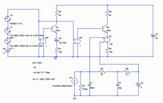
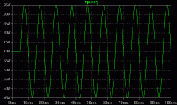
The simulation circuit looks like this. Some things change slightly between the simulations, like the signal sources.
The circuit consists of two CE stages with the same input signal and the same Q point. The one to the right has no thermal effects, while the one to the right uses Anlis model for a TO-92 package (but without heat sink).
The thermal effect is inserted as a voltage source at the emitter, which should be considered part of the Vbe. That is, Vbe is measured from base to the top end of the emitter resistor. The circuit on the left has a fixed voltage corresponding to the Q point of the right circuit, so both circuits behave the same if temperature is constant. Power is computed as the C-E voltage of the right transistor multiplied by its Ic, resulting in a current from the current source B1. This current is filtered by a network modelling the thermal impedance. There are a few minor errors here, for simplicity and to make simulations work, but they are very minor. Howver, only thermal effect of the transfer function is simulated. hFE is not affected, but for these circuits it doesn't matter.
Attachments
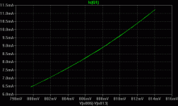
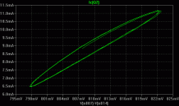
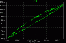
While the right circuit clearly shows how the "Q point" wanders around with the varying temperature, and the HF signals seems to be modulated around a point following the ellipsis.
Clearly the transistor parameters change all the time, and thus the character of the distorsion. However, let's not be deluded by the boring figure for the nonthermal case. We do slide up and down along the transfer curve also there, which makes the parameters and thus also the distorsion spectrum change. The difference is, that in the nonthermal case the follow a curved line forth and back, so the parameters change in the same way in both directions (although in reversed order, of course). In the thermal case, we instead go around in a loop, so we have a different sequence of paramater changes for increasing input signal than for decreasing input signal. That is, the changes in distorsion character will be different when "going up" and "going down".
Clearly the transistor parameters change all the time, and thus the character of the distorsion. However, let's not be deluded by the boring figure for the nonthermal case. We do slide up and down along the transfer curve also there, which makes the parameters and thus also the distorsion spectrum change. The difference is, that in the nonthermal case the follow a curved line forth and back, so the parameters change in the same way in both directions (although in reversed order, of course). In the thermal case, we instead go around in a loop, so we have a different sequence of paramater changes for increasing input signal than for decreasing input signal. That is, the changes in distorsion character will be different when "going up" and "going down".
Attachments
Extremely interesting !
Your transistor model can't be 100% exact, but I'd say it is exact enough to estimate the "order of magnitude" of things ; and the error caused by thermal "hysteresis" appears to be quantitatively on the same order, or even larger, than the error caused by the transistor's transfer function nonlinearity.
Now, I wonder what this will do to a complete amplifier (with feedback) ; the DC operating point will probably be a bit "randomized"... I'll try to run some sims too.
However in a diff amp, both transistors should heat and cool about the same since they have the same Vce and delta Ic is small. We'd see modulation of the diff amp gain, though, but I'm not so sure about its offset. (Unless the amp clips : in this case, you get large delta Pdissipated).
But think about an amp as a whole, not just parts.
Diff pair -> VAS -> Buffer -> Output
Let's call the "control signal" the signal the diff pair has to send the rest of the amp to control it. It's the feedback error signal, more or less diff pair offset and nasties.
I think it would be interesting to first, measure this control signal without thermal modeling.
Then, to measure this signal with thermal models of the VAS, buffer and outputs applied.
I'm thinking about that because diff pairs are only perfect when the diff voltage is zero, which never happens in the real world, of course. As shown by D. Self, a slight imbalance of the diff pair is enough to significantly worsen distortion.
So, I wonder if the control signal needed to correct thermal effects in the VAS and output could be larger than the one needed to reproduce the input signal (music). In that case, IMD comes.
Peufeu,
That distortion - thermal or transfer - cannot occur in the ltp if the Vbe of both devices does not vary....... If operating in constant power, any displacement in inputs can only result in a linear transfer function, due entirely to the purely ohmic degeneration.
Cheers,
Hugh
That distortion - thermal or transfer - cannot occur in the ltp if the Vbe of both devices does not vary....... If operating in constant power, any displacement in inputs can only result in a linear transfer function, due entirely to the purely ohmic degeneration.
Cheers,
Hugh
Peufeu,
yes there is a lot more one could an should do. The point of my exercise was not primarly to get quantitative measures but only to characterize the behaviour qualitatively. However, as you say, I also think my simulations give a rough estimate of the quantitative measures. In fact, the thermal distorsion in this case seems to be much worse than I had expected.
Neither was the point of the exercise to investiga any particular type of amp, but only to show the effect in a case where it seems to occur. That is, I deliberately did not try to minimize or get rid of thermal problems here, but rather use a straightforward gain stage. Just as jcx pointed out, I think we now how to get rid of thermal problem; just make sure we minimize the power variation in the input devices sufficiently by whatever method. However, even if we know how to minimize thermal distorsion, it is still interesting to know if it exists at all. Otherwise there is no need to minimize it. It is also interesting to figure out the character of thermal distorsion.
I added a third gain stage, identical to the second one but with thermal feedback from the second stage, not from itself, and with the base held at constant voltage. This would thus correspond to my suggested experiment using a dual transistor where one is active and the other is idle but affected by the thermal drifts in the active one.
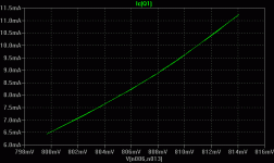
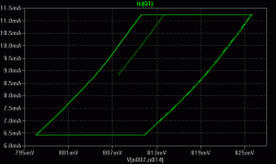
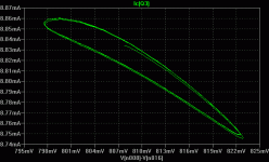
First the Vbe-Ic diagram of the idle transistor when the active one is fed the transient sine wave as input. What we see is just the drift of the Q point in the idle transistor as an effect of varying temperature in the acitve one. Do note, however, that the simulation assumes a perfect thermal coupling between the devices.
It shows a similar character as the diagram for the active transistor posted earlier and presumably we should expect something similar, although perhas at a different magnitude, from the suggested experiment.
Attachments
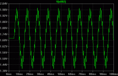
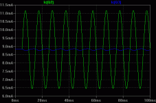
And this is Ic in the active stage (green) and the idle one (blue). That is, the blue curve is the Ic variation in a transistor with no input signal, but thermally coupled to the active one. The magnitude of the blue curve is some 2-3 % of that for the green curve.
Of course, there are many errors and uncertainties in this simulation, but I think it should be on the right order of magnitude, at least. Also note that all these simulations depend on the frequencies involved due to the filtering effects of the thermal impedances. I have somewhat arbitrarily picked frequencies within the audio band that show a clear thermal distorsion behaviour.
Of course, there are many errors and uncertainties in this simulation, but I think it should be on the right order of magnitude, at least. Also note that all these simulations depend on the frequencies involved due to the filtering effects of the thermal impedances. I have somewhat arbitrarily picked frequencies within the audio band that show a clear thermal distorsion behaviour.
Attachments
Hi Charles.
I have now.")
I didn't bother with it earlier since I was mostly interested in the transient behaviour and I cannot quite see how to do a meaningful FFT for that.
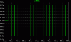
I did a run now, though, of the steady state behaviour using a 100 Hz sine as input.
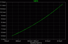
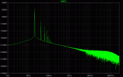
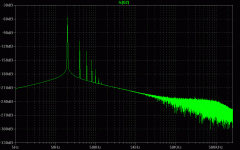
The first diagram is Ic of the transistor with no thermal effects, ie. with no thermal distorsion.
phase_accurate said:Hi Christer
Have you performed any FFT in order to see what the actual distortion caused by the thermal effects looks like ?
I have now.
I didn't bother with it earlier since I was mostly interested in the transient behaviour and I cannot quite see how to do a meaningful FFT for that.
I did a run now, though, of the steady state behaviour using a 100 Hz sine as input.
The first diagram is Ic of the transistor with no thermal effects, ie. with no thermal distorsion.
Attachments
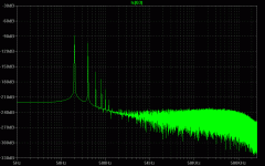
And this is an FFT for the Ic drift in the idle transistor that is thermally coupled to the previous one. This should correspond roughly to the actual thermal component of the previous diagram. Note that this is only a distorsion signal, so the fundamental is not really the signal fundamental but a distorsion component at the fundamental frequency.
Attachments
- Status
- This old topic is closed. If you want to reopen this topic, contact a moderator using the "Report Post" button.
- Home
- Amplifiers
- Solid State
- Memory Distortion? and some new beginnings.