Millwood
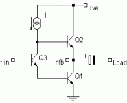
I am now able, somewhat belatedly, to reply to your post #595 (on page 40) in which you state that, in the JLH Class-A, there is no requirement for the gains of the output BJTs to be matched and that optimum performance will be obtained even if the gains of the two output devices are different. This is fallacious, as I will explain. I suspect that you have only considered the small signal situation and have not looked at the broader picture.
I trust you will agree that for true push-pull working in a Class-A output stage, one output device turns off as the other turns on, the net result being that the maximum current that can be supplied to the load is twice the quiescent current.
Referring to the simplified schematic (I have attached it again to save you going back to my original post), let’s assume that the quiescent current is 1A and that the gains of Q1 and Q2 are both 100. I am also assuming at this stage that Q3 is working as a perfect current phase splitter.
With no signal present:
Ib1 = 1/100 = 10mA
Ib2 = 1/(100+1) = 9.9mA
I1 will therefore be 19.9mA
The maximum available current swing due an input signal is when one or other of the base currents reaches zero. When this happens we have:
Ib1 = 0
Ib2 = 19.9mA
Ic1 = 0
Ie2 = 0.0199*(100+1) = 2A
Iout = Ie2 – Ic1 = 2A
Or:
Ib1 = 19.9mA
Ib2 = 0
Ic1 = 0.0199*100 = 1.99A
Ie2 = 0
Iout = -1.99A
Therefore the peak output current is (as near as dammit) twice the quiescent current and true push-pull working is obtained.
Now let’s see what happens if the gains of the output transistors are not equal. We’ll keep Q1 at 100 and make Q2 150. The quiescent current is still 1A
With no signal present:
Ib1 = 1/100 = 10mA
Ib2 = 1/(150+1) = 6.63mA
I1 will therefore be 16.63mA
As before, the maximum available current swing due an input signal is when one or other of the base currents reaches zero. When this happens we have:
Ib1 = 0
Ib2 = 16.63mA
Ic1 = 0
Ie2 = 0.01663*(150+1) = 2.51A
Iout = Ie2 – Ic1 = 2.51A
Or:
Ib1 = 16.63mA
Ib2 = 0
Ic1 = 0.01663*100 = 1.633A
Ie2 = 0
Iout = -1.633A
As you will see, the maximum output current (for a symmetrical swing) is now significantly less than twice the quiescent current. As a result, to achieve the same peak output current, if unmatched transistors are used the quiescent current must be increased beyond that required for matched devices, with the corresponding decrease in efficiency.
You can check using other gain figures, but you will find that the greater the gain difference between the output transistor the lower the available peak output current for a given quiescent current and the greater the deviation from ‘ideal’ push-pull working.
The foregoing is to a certain extent academic in that it assumes perfect current phase splitting, and uses greatly simplified calculations. Extensive simulation over several years using a variety of output transistor models has indicated to me that the peak output current from a JLH Class-A will be between 1.3 and 1.6 times the quiescent current, depending on the output devices used. This assumes perfectly matched transistors.
Simulation also reveals that the peak output current reduces, for a given quiescent current, if the gains of the two transistors differ. If the gains differ too much, the benefits of push-pull working may be lost completely. For example, if Q1 has a gain of 95 and Q2 is a poor transistor with a gain of only 50, simulation indicates that the maximum (symmetrical) output current equals the quiescent current. If the gain variation is extreme (say 175 and 50) the peak output current is actually less than the quiescent current, in which case it would be better to use a single-ended circuit.
Geoff
Attachments
I needed to rush out for lunch (yeah, at 4pm,  ) so I will make this quick.
I think we have a difference in definition. You define "optimum" as high efficiency while no distortion (in this particular case).
I defined optimum as no distortion. As you can go through my proof (in this post: http://www.diyaudio.com/forums/showthread.php?postid=285198#post285198) whereby equation 5) explicitly states that the output current, Il, is a coefficient times the input signal. The magnitude of that coefficient is directly tied to betas of both upper and lower device.
But the Il is perfectly in sync with the input signal -> no distortion.
) so I will make this quick.Geoff said:I am now able, somewhat belatedly, to reply to your post #595 (on page 40) in which you state that, in the JLH Class-A, there is no requirement for the gains of the output BJTs to be matched and that optimum performance will be obtained even if the gains of the two output devices are different. This is fallacious, as I will explain.
As you will see, the maximum output current (for a symmetrical swing) is now significantly less than twice the quiescent current. As a result, to achieve the same peak output current, if unmatched transistors are used the quiescent current must be increased beyond that required for matched devices, with the corresponding decrease in efficiency.Geoff
I think we have a difference in definition. You define "optimum" as high efficiency while no distortion (in this particular case).
I defined optimum as no distortion. As you can go through my proof (in this post: http://www.diyaudio.com/forums/showthread.php?postid=285198#post285198) whereby equation 5) explicitly states that the output current, Il, is a coefficient times the input signal. The magnitude of that coefficient is directly tied to betas of both upper and lower device.
But the Il is perfectly in sync with the input signal -> no distortion.
I just started my listening test of my pair of MOSFETs JLH 10W Class A amplifiers....
. oooohhhhhhfffffffffffff the sound stage is soooooooooooooooooo much better than my original BJT version..
I was chocked realy... I'm really really very euforic on this one.. it's so nice to have that 'virtual live performance quality' .. the soundstage covers allmost my whole back wall...
after several days of simulating, buying parts, blowing MOSFETs, failing soldering iron, discussing the circuit, again simulating alll night, measureing on scope, optimizing, again simulating, again blowing MOSFETs, again buying parts... .. but it was worth while..
The only problem I have now is that I can't say ' well it must be the MOSFET output stage being so superoir' .. because I used different parts, and gain sturcture.... so many factor have changed that I can't claim the MOSFETs must be the reason why it is so much better... I also spend far more time optimizing on this one that on my BJT version..
I will attache the circuit I have used for my version. I sound very very good, soundstage is fabulous, tembre sound good, but I thinks that more difficultto judge....
Thanks Millwood for the inspiration!
PS
the 6.8uF is a Non Polarized capacitor froman old crossover network
.
oooohhhhhhfffffffffffff the sound stage is soooooooooooooooooo much better than my original BJT version.. I was chocked realy... I'm really really very euforic on this one.. it's so nice to have that 'virtual live performance quality' .. the soundstage covers allmost my whole back wall...
after several days of simulating, buying parts, blowing MOSFETs, failing soldering iron, discussing the circuit, again simulating alll night, measureing on scope, optimizing, again simulating, again blowing MOSFETs, again buying parts... .. but it was worth while..
The only problem I have now is that I can't say ' well it must be the MOSFET output stage being so superoir' .. because I used different parts, and gain sturcture.... so many factor have changed that I can't claim the MOSFETs must be the reason why it is so much better... I also spend far more time optimizing on this one that on my BJT version..
I will attache the circuit I have used for my version. I sound very very good, soundstage is fabulous, tembre sound good, but I thinks that more difficultto judge....
Thanks Millwood for the inspiration!
PS
the 6.8uF is a Non Polarized capacitor froman old crossover network
Attachments
tschrama said:I just started my listening test of my pair of MOSFETs JLH 10W Class A amplifiers....
Nice to know that you liked it.
tschrama said:I will attache the circuit I have used for my version. I sound very very good, soundstage is fabulous, tembre sound good, but I thinks that more difficultto judge....
my version has much higher Iq in the driver stage then yours. I think that's the biggest differernce between our versions.
Thanks Millwood for the inspiration![/B][/QUOTE]
You are welcome. I think it is more of a coorperation than anything else.
my next project is to built a 5 or 6 channel one and then prototype the complementory MOSFET JLH1969,
Millwood
You have obviously missed the point. Perhaps a break for lunch will bring some more understanding. Unless, of course, you believe that an output stage which has a maximum load current equal to the quiescent current is operating in push-pull.
You refer to distortion and the fact (sorry, your assertion) that it is not affected by the use of unmatched output transistors. Have you actually read Table 2 of the original 1969 article which gives the results of THD measurements for matched and unmatched output devices?
Geoff
Geoff said:Unless, of course, you believe that an output stage which has a maximum load current equal to the quiescent current is operating in push-pull.
I don't recall me stating that.
Geoff said:You refer to distortion and the fact (sorry, your assertion) that it is not affected by the use of unmatched output transistors. Have you actually read Table 2 of the original 1969 article which gives the results of THD measurements for matched and unmatched output devices?
Geoff
Yes, I have. all I am saying in this "academic" exercise is that 1) gain matching isn't required for this to work; 2) in theory, this circuitry does not require gain matching; 3) it does not require the current matching that x-pro and you had indicated.
if you are interested in a constructive discussion, I would love to hear your view. Otherwise, I suggest that you leave your attitude at home.
Hi Millwood,
ActuallyI think the standing current in the driver stage is an minor detail. The current in it self doesn't help anything, but the lower driver resistors (needed for higher current) help speeding up the circuit as you have shown in simlations. But since the speed of the circuit is high anyway, going from 1MHz to 2MHz bandwidth is not nessecerraly an improvement.
What is important , is that both output devices stay in exact anti-phase. This a also invluenced by the gate-snoopers. Their value is importand and not equal: upper 150 Ohm being the minimum for stable operation, lower 820 for equal bandwidth.
Further more the high and equal source resistors (0.5R because I only had 5 1R resistors, so 0.33R wasn't possible) and the equal driver resistors (470R) garantee allmost perfect current sharing.
Than the 270pF compensation cap is neccesery to reduce overshoot. Such a compensation cap can be placed at different nodes in the circuit, but this place achieves most symmetric and highet slewrate wihtout overshoot (the 100KHz square wave looks perfect allthough a bit rounded) .
As I am typing now anyway, I will point out some more design issues:
The 4.7uF input bias cap is choosen to speed up the turn-on-bump (now only a few ms).
The 100uF bootstrap cap is choosen large to garantee the correct phase relationship of the upper/lower output current. Choosing this too small causes significant currentto cross-conduct from upper output device to lower output device.
Input resistor 10K is choosen a bit low to limmit output to input couping, which can causes oscilation.
Well that's about it .... any questions.. please ask
Best regards,
Thijs
PS
be nice to Geoff... I'm sure there's no attitude involved..
my version has much higher Iq in the driver stage then yours. I think that's the biggest differernce between our versions
ActuallyI think the standing current in the driver stage is an minor detail. The current in it self doesn't help anything, but the lower driver resistors (needed for higher current) help speeding up the circuit as you have shown in simlations. But since the speed of the circuit is high anyway, going from 1MHz to 2MHz bandwidth is not nessecerraly an improvement.
What is important , is that both output devices stay in exact anti-phase. This a also invluenced by the gate-snoopers. Their value is importand and not equal: upper 150 Ohm being the minimum for stable operation, lower 820 for equal bandwidth.
Further more the high and equal source resistors (0.5R because I only had 5 1R resistors, so 0.33R wasn't possible) and the equal driver resistors (470R) garantee allmost perfect current sharing.
Than the 270pF compensation cap is neccesery to reduce overshoot. Such a compensation cap can be placed at different nodes in the circuit, but this place achieves most symmetric and highet slewrate wihtout overshoot (the 100KHz square wave looks perfect allthough a bit rounded) .
As I am typing now anyway, I will point out some more design issues:
The 4.7uF input bias cap is choosen to speed up the turn-on-bump (now only a few ms).
The 100uF bootstrap cap is choosen large to garantee the correct phase relationship of the upper/lower output current. Choosing this too small causes significant currentto cross-conduct from upper output device to lower output device.
Input resistor 10K is choosen a bit low to limmit output to input couping, which can causes oscilation.
Well that's about it .... any questions.. please ask
Best regards,
Thijs
PS
be nice to Geoff... I'm sure there's no attitude involved..
Geoff said:Millwood
You have obviously missed the point. Perhaps a break for lunch will bring some more understanding. Unless, of course, you believe that an output stage which has a maximum load current equal to the quiescent current is operating in push-pull.
You refer to distortion and the fact (sorry, your assertion) that it is not affected by the use of unmatched output transistors. Have you actually read Table 2 of the original 1969 article which gives the results of THD measurements for matched and unmatched output devices?
Geoff
Geoff,
they both probably like SE approach and sound
. There is nothing wrong in liking SE sound but I think they both somewhat confused as to what difference between SE and PP is. x-pro
Hi All,
Anyone. How can I store a reply page so that I don't lose it every time I go back to check an entry that I am writing about ?
Limited reply here, because of this.
POST 673. Hi tschrama.
I might consider Mosfets if I was not already so happy with a modified bipolar JLH. Will look at your circuit again shortly, esp with regard to the 270pF C6, which is bound to make it sound smooth, but maybe not accurate.
I use 2SC5200 outputs, and where you have 470R for both R5 and R13, I use 390R. There is less output power from Mosfets, though they will automatically run into class-AB in the JLH circuit.
Hi Geoff. Nicely written. (I dare not go back to find Post number, or I'll lose this.)
Of course the distortion is lowest when the devices are closely matched; that's one of the fundamental principles of class-A push-pull, also why the JLH is so clean at lower reproduction levels.
Can I add that distortion is lower again when the bootstrapped collector resistor and the emitter resistor at the current splitter are also equal, as Tschrama has done with his 470Rs.
I have another way of stating the unavoidable 1.3 to 1.6 quiescent/peak ratio figure, which is due to increased gain droop within hot power bipolars;
that is to think of the standing bias requirement as being 0.75 of peak for resistive or full-range single driver loading, or Iq=Ip for driving multi-driver hi-fi loudspeaker systems which have unavoidable loudspeaker impedance dips.
POST 675. Hi Caleby.
Smaller pcb in middle. That would be my choice, with say input transistor (at bottom of picture) and its screened cable going to an *insulated* input socket. I would also have a star earth at other side (top of picture) of your board (individually soldered solder tags bolted tightly together) . To extend output wires I use solid copper house wiring or coloured three phase, which can be bent into a shape it will hold permanently. I tend to go for 1/4 to 3/8 inch spacing between B_C_E wires and any metalwork, don't twist or lace together. I also bolt my output devices directly to their heatsinks, then I insulate these by oversize drilling the chassis mounting holes and insert short cut lengths of fish tank air pipe as concentric spacers.
Must go. Back later ............ Graham.
Hi X-pro,
LOL

I was convinced that the MOSFET version wouldn'twork etc ect ect, but Millwood pushed on so I kept on thinking, simulating and perhapts most improtantly drawring with pen and paper untill I understood....
A MOSFET JLH 10w Class A works in perfect Push-Pull.
One more time... please take a close look at the schematic while I explain...
Because the current that passes through the lower driver-resistor (470R my last schematic) must also flow through the upper driver resistor (also 470R in my last schematic).
So (drive-resistor) voltage drop across the driver-resistors is equal..
Since the lower MOSFETs' source is tied to ground, this voltage drop is all it drives
For the upper MOSFET is becomes a bit more difficult to see, but the 'not-really-a-bootstrap' capacitor is acting as a voltage source, it dictates that the upper node of the upper driver-resistor must followe the output AC voltage.. since the gate is tied to the lower-end of the upper driver-resistor, the same drive-voltage that drives the lower MOSFET, is super impossed on that, in effect both MOSFETs are driven equally in anti-phase ...
For this to happen
1]both the driver-resistors must be of equal value, and
2]both MOSFETs must has equal transductance ( 0.5R source resistance helpt but not really nessecery)...
3]The 'not-realy-a-bootstrap' capacitor must act as voltage source, so it impedance must be << 766R at all frequencies..
I am quiete convinced that I'm not mistaken, I've simulated it, build it, and measured it, this is how it works..It even sounds good
Best regards,
Thijs
LOL
I was convinced that the MOSFET version wouldn'twork etc ect ect, but Millwood pushed on so I kept on thinking, simulating and perhapts most improtantly drawring with pen and paper untill I understood....
A MOSFET JLH 10w Class A works in perfect Push-Pull.
One more time... please take a close look at the schematic while I explain...
Because the current that passes through the lower driver-resistor (470R my last schematic) must also flow through the upper driver resistor (also 470R in my last schematic).
So (drive-resistor) voltage drop across the driver-resistors is equal..
Since the lower MOSFETs' source is tied to ground, this voltage drop is all it drives
For the upper MOSFET is becomes a bit more difficult to see, but the 'not-really-a-bootstrap' capacitor is acting as a voltage source, it dictates that the upper node of the upper driver-resistor must followe the output AC voltage.. since the gate is tied to the lower-end of the upper driver-resistor, the same drive-voltage that drives the lower MOSFET, is super impossed on that, in effect both MOSFETs are driven equally in anti-phase ...
For this to happen
1]both the driver-resistors must be of equal value, and
2]both MOSFETs must has equal transductance ( 0.5R source resistance helpt but not really nessecery)...
3]The 'not-realy-a-bootstrap' capacitor must act as voltage source, so it impedance must be << 766R at all frequencies..
I am quiete convinced that I'm not mistaken, I've simulated it, build it, and measured it, this is how it works..It even sounds good
Best regards,
Thijs
I use 2SC5200 outputs, and where you have 470R for both R5 and R13, I use 390R. There is less output power from Mosfets, though they will automatically run into class-AB in the JLH circuit.
Indeed there's a view volts (about 3) less drive availeble in the MOSFET version. But like you said: there is a big advantage of the MOSFET version too: it will shift from class A to class AB if more current is asked for. This is not availeble with the BJT version at least not to that extent.
Best regards,
Thijs
(I allways have the thread opend in 2 windows, 1 reply window, and a second to keep viewing the thread.. maybe this could help you too)
tschrama said:This a also invluenced by the gate-snoopers. Their value is importand and not equal: upper 150 Ohm being the minimum for stable operation, lower 820 for equal bandwidth.
I suspect that what the higher gate stopper does is to slow the lower mosfet down so that the whole output stage works more as a common emitter than a common collector configuration.
tschrama said:Further more the high and equal source resistors (0.5R because I only had 5 1R resistors, so 0.33R wasn't possible) and the equal driver resistors (470R) garantee allmost perfect current sharing.
I am still of the view that there is no need for "perfect" current sharing, either in the original jlh or this modification.
Graham Maynard said:There is less output power from Mosfets, though they will automatically run into class-AB in the JLH circuit.
I never understood this when tschrama mentioned it a while ago. When overdriven, the BJT version will go into class ab as well: a hugely positive signal will shut off the lower bjt. The same is true here with the mosfet version. so what's so unique about the mosfet version?
Graham Maynard said:that's one of the fundamental principles of class-A push-pull,
so what exactly are all of those "fundamental principles" of class-a push-pull? Why don't we list them all out here so we all have a common frame of referrence? BTW, why are they "foundamental" to a class-a push-pull? and what referrence do you have that says they are indeed foundamental?
tschrama said:both MOSFETs are driven equally in anti-phase ...
this, in my view, is the single biggest assumption and potential problem area for the jlh design. Because of the output asymmetry from the driver (higher Zout on the upper end than on the lower end), any device with high output capacitance (the driver), or input capacitance (the output devices) can cause large phase shifting between the upper and lower output. This is where MOSFET has output devices have a decidedly disadvantage over BJT.
the "cure" is to run higher current through the driver, like I did. However that has its own evil: it tends to overload the input transistor.
All of this, I think, calls for a MOSFET driver stage. The mosfet has to be a small signal or medium power mosfet with small input capacitance (and its variance) and high current capabilities. I am looking into some fairchild mosfets to see if I can find one that works.
I suspect that what the higher gate stopper does is to slow the lower mosfet down so that the whole output stage works more as a common emitter than a common collector configuration.
Actually the purpuse is to garatee equale drive impedance, compensating the different output impedance of the driver output. This causes major cross-conduction spikes at HF (sims and measurements agree once more) ..
Because of the output asymmetry from the driver (higher Zout on the upper end than on the lower end), any device with high output capacitance (the driver), or input capacitance (the output devices) can cause large phase shifting between the upper and lower output. This is where MOSFET has output devices have a decidedly disadvantage over BJT.
The different gate-snoopers take perfectly care of this problem. Even with this increased gate-snooper,the MOSFET as faster than my 2N3055.
the "cure" is to run higher current through the driver, like I did. However that has its own evil: it tends to overload the input transistor.
Well, a partial cure is to decrease the source impedance, the associated increase in driver current is just a side effect. Still: lower impedance doesn't help much. Actually you are moving the same problem to a higher frequency, just as severe, but more dangerous. You really have to balance them with different gate-snoopers.
I never understood this when tschrama mentioned it a while ago. When overdriven, the BJT version will go into class ab as well: a hugely positive signal will shut off the lower bjt. The same is true here with the mosfet version. so what's so unique about the mosfet version?
Sadly, the BJT does not run into class AB, it tries, but succeed only marginally. The input impedance of the 2N3055s being the cullprit, hence the MOSFETs go into class AB very smoothly indeed.
Can you comment on your perceived sound quality Millwood? I being very very happy with mine so far..
Best regards,
Thijs
tschrama said:Can you comment on your perceived sound quality Millwood? I being very very happy with mine so far..
Best regards,
Thijs
I never heard of the BJT version so I have no basis for comparison. And so far, I have only one module running so hard to say anything about soundstage,
.I compared mine with three other amps. a parasound (80wx5), a H/K signature (100wx5), and a sony (120wx5). all of the commercial amps can run much louder than the jlh for obivious reasons. When running comparable volume levels, the jlh has about the same performance of the commercial amps. However, it is in bass where the jlh excels: it is very lively, 'effortless' as my wife called it. the commercial amps appear a little "dry" in bass. Of them, the parasound comes closest to the jlh, and the sony the worst.
I have it turned on in my garage when I am in it, and in my (highly biased) view, I don't get tired listening to it. It sounded very melow (?).
It is driven a PSB alpha (4-6ohm, quite inefficient speaker) and does a good job filling my garage of about 8 meters by 6 meters, if I tune up the volume.
I have it right now biased at about 1amp. How about yours?
Hi Millwood,
I have set my amps to 500mA idle. This not as high as I would like to, but I have not larger heat sink and absolutely no money to buy a larger one. At 1000mA (2 channels, 1 heatsink ) things get really hot allready. I hardly ever usemore than 1 Watt of power so I'm not that worried, but still...
I *think* I can hear a difference in sound quality as I reduce idle current below 800mA (2 channels). The sound get thin,and sound stage narows a bit. I agree with the bass quality, but maybe my BJT is just as good or even better as it. The front-to-back depth is also very good on my amps. (I'm biased too ). Maybe I could bold serveral small heatsink to the one a use now and increase idle current even more...
Greetings,
Thijs
I have set my amps to 500mA idle. This not as high as I would like to, but I have not larger heat sink and absolutely no money to buy a larger one. At 1000mA (2 channels, 1 heatsink
) things get really hot allready. I hardly ever usemore than 1 Watt of power so I'm not that worried, but still...I *think* I can hear a difference in sound quality as I reduce idle current below 800mA (2 channels). The sound get thin,and sound stage narows a bit. I agree with the bass quality, but maybe my BJT is just as good or even better as it. The front-to-back depth is also very good on my amps. (I'm biased too
). Maybe I could bold serveral small heatsink to the one a use now and increase idle current even more... Greetings,
Thijs
- Home
- Amplifiers
- Solid State
- JLH 10 Watt class A amplifier