I tried it on the original jlh bjt. the lower bjt is working but not the upper bjt: it was either turned full on or full off. I used two perfect current source of 40ma each. I need to figure out why.
Note that the output BJT eat significant base-current.. so the two current source can not be equal. In the original version the upper resistor draw 40mA, but the lower 300uA.. the rest is flowing through the bases of the two output BJT... Further more the lower driver resisotor is only there to increase the standing current through the driver .. is has practically not invluence on AC current...
I allways use some high resistor parrallel to a perfect-CCS to keep my sim from crashing or giving all kinds of weird effects...something like 40k/100k.. but it doesn't seem to be nessecery now..
I used 42mA and 1mA CCS and it works.. no big improvement yet.. I guess it needs a bit of tweaking..
I could also be that the open-loop lineairity is just as good as it can be and the only improvement is to increase open-loop gain...
regards,
Thijs
tschrama said:my sims tell me that for optimum current sharing between the MOSFETS you need the make the upper-driver-resistor 0.85 * value of the lower-driver-resistor
In my circuit this means 850 Ohm upper, 1000Ohm lower..
I swapped the resistors in my simulation and having a higher upper resistor yielded slightly better THD. But I will investigate later.
Chris,
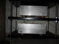
The amps are the ESL ones with the modification of the feedback takeoff point. I tried the C4 mods and did not like the DC offset effects. Since I installed jumpers for those mods they were easy to reverse.
the Amps are not Ballanced but this is a thing I would like to try
so I put the connector just in case.
The hole below the connector hides a socket for power control
enabling to switch to standby mode from the preamp.
I do not use it since I had no time to modify the pre, I'm currently
busy with finishing the speakers for the system.
The Amps sound very open and detailed with a kind of velvety
accent. with some CDs I have I get a feeling the sound stage
extends outside the speakers. I did not expirience this with other systems I heared.
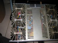
The power supply does not use regulators. I used a circuit Geoff sent me, I think similar ones are posted here.
I used 330 VA Thoroids feeding 50000uF Caps with 100n bypass.
No PS noise I could here, but I use 88db speakers.
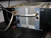
The speaker contacts go through a relay with a delay and external control circuit, powered from a small 12v ps.
This prevents the initial DC offset variation from going to the speaker, I get around 2mv when the amps are warm.
There are allso provisions for clipping indication, does not show very well on thi pics. It's just above the power indicator.
I did not put the circuiet in yet.
The amps are the ESL ones with the modification of the feedback takeoff point. I tried the C4 mods and did not like the DC offset effects. Since I installed jumpers for those mods they were easy to reverse.
the Amps are not Ballanced but this is a thing I would like to try
so I put the connector just in case.
The hole below the connector hides a socket for power control
enabling to switch to standby mode from the preamp.
I do not use it since I had no time to modify the pre, I'm currently
busy with finishing the speakers for the system.
The Amps sound very open and detailed with a kind of velvety
accent. with some CDs I have I get a feeling the sound stage
extends outside the speakers. I did not expirience this with other systems I heared.
The power supply does not use regulators. I used a circuit Geoff sent me, I think similar ones are posted here.
I used 330 VA Thoroids feeding 50000uF Caps with 100n bypass.
No PS noise I could here, but I use 88db speakers.
The speaker contacts go through a relay with a delay and external control circuit, powered from a small 12v ps.
This prevents the initial DC offset variation from going to the speaker, I get around 2mv when the amps are warm.
There are allso provisions for clipping indication, does not show very well on thi pics. It's just above the power indicator.
I did not put the circuiet in yet.
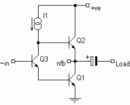
x-pro said:Your circuit loses a main attraction of JLH - it's symmetry. JLH is a proper push-pull circuit, working on the balance of the currents, as output bipolar transistors controlled by their respective base currents, and the driver redistributes the currents according to the signal.
x-pro (Alex)
I thought about this in the last week and did more simulations and here is my thoughts.
1) for the JLH to work, it does not need to be able to perfectly redistribute current between the upper and lower output devices, nor does it need the gins of the output devices to be equal.
the output current on the load is essentially the difference between the emitter current of the upper output and collector current of the lower output. so for the output current to resemble the signal on the base of the driver transistor, you need the following to be true: the base current must be completely out of phase. They can be off in magnitude, as that only impacts the (absolute) magnitude of the output current.
2) in the original JLH1969, the base currents on the two output devices are never the same but they are completely out of phase.
3) I am coming to the realization that the bootstrap on the driver may not be necessary. I took the bootstrap cap off last night and it sounded just as well. Also in simulation it lowered THD as well.
millwood said:3) I am coming to the realization that the bootstrap on the driver may not be necessary. I took the bootstrap cap off last night and it sounded just as well. Also in simulation it lowered THD as well.
the "problem" with this approach is that it considerably lowers the gain of the upper output devices and making the whole amp closer to an "SE" amp.
But in terms of overall performance of the amp, there is no problem whatsoever.
millwood said:3) I am coming to the realization that the bootstrap on the driver may not be necessary. I took the bootstrap cap off last night and it sounded just as well. Also in simulation it lowered THD as well.
this might be desirable for those who want to listen to low-open loop gain amps.
Hi Millwood,
I have some more time to think things over too. I think I'm coming to a point where I really understand the original and your topolgy.
As stated in the original 1969 article/replies/follow up, that is true.
But open loop liniarity will be best when both output BJTs have equal Hfe. The effect of slightly differing Hfe has been investicated by JLH him self and published in 1995 (? ).. Check the 'Class-A website' .
If the Hfe is equal, than the quesient base-current must be equal. The AC base-current are very equal, only a the slight difference due to the added base-current of the driver. But this is partly compensated by the lower-driver-resistor (2k2), which set the Iq of the drivers a bit higher and eats a bit AC current too. But we are talking uA here.
It's not a bootstrap any more, since inyour topoly it passes singnificant current. But the 'not-really-a-bootstrap' arangment makes it easy to set bias current through the output MOSFETS and still maintain optimum current-balancing. Setting this balance off is make the output-power, efficinety and openloop linearity suffer, but maybe you get a bit higher openloop gain. I have to run a sim as well to confirm this.
[edit: so I did.. I was errorous.. It lower open loop gain about 8 dB. I can fing not decreasing THD in my sims, but I did find that the amp indeed now functions more like a SE-amp and output power is NOT decreased.. it still becomes more interesting everyday") )
)
Further more I have come to the conclusion that the original is current-driven and your ealier post of being it voltage driven just as well, does not really take into accout the driving- and source- impedance of the various nodes.
The lower output BJT is driven from a relative high inpedance, it's base having only about 2 Ohm inpedance: so it's current driven. It's output to the Speaker load is vias it's collector: also cleary a high impedance node.
The upper output BTJ is driven from collector and the bootstrap, both realtive high impedances. The base draws it current for about 80% from the driver collector and about 20% from the Bootstrap. The base impedanceis about 700 Ohm. This output BTJ must drive a low inpedance: the speaker impedance (8 ohm) is driven for 50% by the lower BTJ, so it looks like a 16Ohm inpedance.. The output inpedance of the upper BTJ is 700/Hfe (about 46,7) or about 15 ohm. ..
Nothing about this original output stage is voltage driven.
Actually the first input stage is a Voltage to current convertor (transimpedance stage), and all following BJT are current driven. the only thing that makes it from a current controlled amplifier to a voltage amplifier is the feedback.
I'm now so enthousiast about this circuit, and your modification, that I decided to build another one: a MOSFET version. Gonna buy the MOSFETs tonight...
I'll be back,
Best regards,
Thijs
I have some more time to think things over too. I think I'm coming to a point where I really understand the original and your topolgy.
1) for the JLH to work, it does not need to be able to perfectly redistribute current between the upper and lower output devices, nor does it need the gins of the output devices to be equal.
As stated in the original 1969 article/replies/follow up, that is true.
But open loop liniarity will be best when both output BJTs have equal Hfe. The effect of slightly differing Hfe has been investicated by JLH him self and published in 1995 (? ).. Check the 'Class-A website' .
2) in the original JLH1969, the base currents on the two output devices are never the same but they are completely out of phase.
If the Hfe is equal, than the quesient base-current must be equal. The AC base-current are very equal, only a the slight difference due to the added base-current of the driver. But this is partly compensated by the lower-driver-resistor (2k2), which set the Iq of the drivers a bit higher and eats a bit AC current too. But we are talking uA here.
3) I am coming to the realization that the bootstrap on the driver may not be necessary. I took the bootstrap cap off last night and it sounded just as well. Also in simulation it lowered THD as well.
It's not a bootstrap any more, since inyour topoly it passes singnificant current. But the 'not-really-a-bootstrap' arangment makes it easy to set bias current through the output MOSFETS and still maintain optimum current-balancing. Setting this balance off is make the output-power, efficinety and openloop linearity suffer, but maybe you get a bit higher openloop gain. I have to run a sim as well to confirm this.
[edit: so I did.. I was errorous.. It lower open loop gain about 8 dB. I can fing not decreasing THD in my sims, but I did find that the amp indeed now functions more like a SE-amp and output power is NOT decreased.. it still becomes more interesting everyday
)Further more I have come to the conclusion that the original is current-driven and your ealier post of being it voltage driven just as well, does not really take into accout the driving- and source- impedance of the various nodes.
The lower output BJT is driven from a relative high inpedance, it's base having only about 2 Ohm inpedance: so it's current driven. It's output to the Speaker load is vias it's collector: also cleary a high impedance node.
The upper output BTJ is driven from collector and the bootstrap, both realtive high impedances. The base draws it current for about 80% from the driver collector and about 20% from the Bootstrap. The base impedanceis about 700 Ohm. This output BTJ must drive a low inpedance: the speaker impedance (8 ohm) is driven for 50% by the lower BTJ, so it looks like a 16Ohm inpedance.. The output inpedance of the upper BTJ is 700/Hfe (about 46,7) or about 15 ohm. ..
Nothing about this original output stage is voltage driven.
Actually the first input stage is a Voltage to current convertor (transimpedance stage), and all following BJT are current driven. the only thing that makes it from a current controlled amplifier to a voltage amplifier is the feedback.
I'm now so enthousiast about this circuit, and your modification, that I decided to build another one: a MOSFET version. Gonna buy the MOSFETs tonight...
I'll be back,
Best regards,
Thijs
tschrama said:I'm now so enthousiast about this circuit, and your modification, that I decided to build another one: a MOSFET version. Gonna buy the MOSFETs tonight...
I look forward to your report.
Millwood
I'm sorry, but your analysis is not strictly correct. Also, you are causing confusion by inferring that the results obtained with your MOSFET output stage (resulting in the fact that your amp is NOT working as a JLH) are applicable to a true JLH Class-A.
Alex and Thijs have already covered this earlier in the thread, but I will repeat the explanation in a slightly different way in an attempt to provide more clarity and understanding.
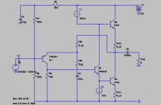
I have included an outline schematic of the basic push-pull Class-A circuit. The circuit operation is as follows, assuming Q1 and Q2 are matched devices and ignoring the effects of Q3 base current. If no signal is present on the base of Q3, the output from the constant current source is split equally between the two output transistors. If an input signal causes Q3 to pass more current, the current into the base of Q1 will be increased. As the circuit is fed from a constant current source, the base current of Q2 will be reduced by the same amount. The converse is true if the input signal causes Q3 to pass less current. Thus Q3 acts as an accurate current phase-splitter and true push-pull output is obtained, provide the gain of the two output transistors is the same.
You are correct that the circuit will continue to work if the current gains of Q1 and Q2 are not the same, or if the phase-splitting action is not as accurate, but optimum performance will not be obtained and distortion will increase. Depending on which output transistor has the higher gain, or in which direction there is an out-of-balance in the phase-splitter, the circuit will work as a common emitter stage with an active collector load or an emitter follower with an active emitter load.
If the constant current source is created by using a bootstrap arrangement, the bootstrap capacitor cannot be removed whilst retaining correct (optimum) circuit operation because there will no longer be a constant current present. You have been able to do so because your amplifier is not working in the push-pull fashion intended in the original design.
If the output BJTs are simply replaced with MOSFETs, the circuit ceases to operate as originally intended since the current phase-splitting action ceases and push-pull operation is no longer available. In order to use MOSFETs whilst retaining the push-pull feature, the current outputs from Q3 must be converted to a voltage to drive the gate by adding a suitable resistor between the gate and the source of each MOSFET.
The statements made in Posts 589, 590 and 591 may well be correct for your non-JLH amp but they are not applicable to a true version of this excellent design.
Geoff
I'm sorry, but your analysis is not strictly correct. Also, you are causing confusion by inferring that the results obtained with your MOSFET output stage (resulting in the fact that your amp is NOT working as a JLH) are applicable to a true JLH Class-A.
Alex and Thijs have already covered this earlier in the thread, but I will repeat the explanation in a slightly different way in an attempt to provide more clarity and understanding.
I have included an outline schematic of the basic push-pull Class-A circuit. The circuit operation is as follows, assuming Q1 and Q2 are matched devices and ignoring the effects of Q3 base current. If no signal is present on the base of Q3, the output from the constant current source is split equally between the two output transistors. If an input signal causes Q3 to pass more current, the current into the base of Q1 will be increased. As the circuit is fed from a constant current source, the base current of Q2 will be reduced by the same amount. The converse is true if the input signal causes Q3 to pass less current. Thus Q3 acts as an accurate current phase-splitter and true push-pull output is obtained, provide the gain of the two output transistors is the same.
You are correct that the circuit will continue to work if the current gains of Q1 and Q2 are not the same, or if the phase-splitting action is not as accurate, but optimum performance will not be obtained and distortion will increase. Depending on which output transistor has the higher gain, or in which direction there is an out-of-balance in the phase-splitter, the circuit will work as a common emitter stage with an active collector load or an emitter follower with an active emitter load.
If the constant current source is created by using a bootstrap arrangement, the bootstrap capacitor cannot be removed whilst retaining correct (optimum) circuit operation because there will no longer be a constant current present. You have been able to do so because your amplifier is not working in the push-pull fashion intended in the original design.
If the output BJTs are simply replaced with MOSFETs, the circuit ceases to operate as originally intended since the current phase-splitting action ceases and push-pull operation is no longer available. In order to use MOSFETs whilst retaining the push-pull feature, the current outputs from Q3 must be converted to a voltage to drive the gate by adding a suitable resistor between the gate and the source of each MOSFET.
The statements made in Posts 589, 590 and 591 may well be correct for your non-JLH amp but they are not applicable to a true version of this excellent design.
Geoff
Attachments
Geoff said:Millwood
I'm sorry, but your analysis is not strictly correct.
I don't disagree with your analysis. All I am asking is that there are alternative views to the same circuitry. and I will expand on that later on.
Geoff said:I have included an outline schematic of the basic push-pull Class-A circuit.
Thus Q3 acts as an accurate current phase-splitter and true push-pull output is obtained, provide the gain of the two output transistors is the same.
I can show that even if the gain of the two output devices are different, you will get a completely accurate signal on the load.
Let's assume that the base current of Q2 is Ib2, and that of Q1 is Ib1 (forget about the fact that I1 is perfect as you can actually relax this. ie. replace with I1 with a resistor and it will still work).
assume the current gain of Q2 is beta2 and Q1 is beta1. so the emitter current of Q2 is
1> Ie2=(beta2+1)*Ib2,
and the collector current of Q1 is
2> Ic1=beta1*Ib1.
the current going to the load,
3> Il=Ie2-Ic1=(beta2+1)*Ib2-beta1*Ib1.
For a perfect phase splitter, we know that Ib2 and Ib1 are out of phase, or
4> Ib1=-k*Ib2 where k is some constant (k=1 in your example). so
5> Il=(beta2+1+k*beta1)Ib1.
and Ib1 is clearly driven by the input signal. so your Il will be simply a constant times that input signal.
Geoff said:as you can see, there is no requirement that beta1=beta2 for the above to be a perfect reproduction of the input. But the phase splitter has to be exactly 180 degrees apart. Otherwise, you can not reduce equation 3> to equation 5> (actually you can show, quite easily, that Il will be a function of Ib1 (or Ib2) and the phase angles and nature of the input singal, if the phase splitter isn't perfect).
and I am reasonably sure that Q1 and Q2 are in push-pull.
Geoff said:You are correct that the circuit will continue to work if the current gains of Q1 and Q2 are not the same, or if the phase-splitting action is not as accurate,
the first half of the above statement is current, and the 2nd half isn't, as shown above.
Geoff said:but optimum performance will not be obtained
you will continue to have optimum performance even if the gains of the two output devices are different.
Geoff said:the current outputs from Q3 must be converted to a voltage to drive the gate by adding a suitable resistor between the gate and the source of each MOSFET.
you can also use a current source to do that.
Geoff said:The statements made in Posts 589, 590 and 591 may well be correct for your non-JLH amp but they are not applicable to a true version of this excellent design.
Geoff
I will stand behind them anyday. And yes, they apply to the original JLH. As a matter of fact, JLH had a schematic of non-bootstraped design in his orignal 1969 article.
the way to look at this is to use the following circuitry (which was implicitly used in earlier discussion).
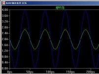
it is essentially your schematic, with the bottom being a current source. You can simulate this and see for yourself that the output will always be the same, as long as the phase splitter is perfect.
You can replace the Q1 (in your diagram) to see what happens when the two output devices have different gains; or you can change the value of I2; or you can insert between I2 and the base of Q1 with a current-controlled current source; or you can replace both output devices with current-controlled current sources and change their coupling coefficients to see how gains impact output.
Attachments
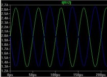
the following is the same graph, after replacing the top current source with a 380ohm resistor. The resistor is selected so that Iq through the top output device is the the same (2a I think).
It is still a push pull, still a perfect sine wave (on the load). Except that now the gain on the top output device is that much lower.
It is still a push pull, still a perfect sine wave (on the load). Except that now the gain on the top output device is that much lower.
Attachments
Hi Geoff and Millwood,
Thanks Geoff for joining us. I'm sure your perspective can contribute a lot on out discussion.
Thanks for taking the effort to keep explaining your views. I'm afraid that my reading and writing skills are not really up to a in-depth analysis of the JHL 1969 circuit.
Interestingly I find myself partly to agree and to disagree with Geoff. Yet I have to read everything twice or more to be able to really understand it... and I find myself disagreing most of Millwood comment.. yet feel unable to point him to the excact error... so maybe I am errorrous..
Geoff and Millwood, would you mind taking another look at the attachment of http://www.diyaudio.com/forums/showthread.php?postid=283519#post283519 and comment on it?
I think the two simplyfied circuits picture the true essence of the original and the MOSFET output stage. It should help us get a final and true understanding of both versions.
Regards,
Thijs
PS I just got 8 IRF540 's to experiment with.. I'll be back
tschrama said:Geoff and Millwood, would you mind taking another look at the attachment of http://www.diyaudio.com/forums/showthread.php?postid=283519#post283519 and comment on it?
the first one is identical to the one I had simulated. It will work, and is a "more" perfect version of the original jlh.
The 2nd one is essentially a mosfet version. Rather than being "current" driven in the BJT world (to borrow your lingo,
), this one is voltage driven. and it will work as well.One way to think about this is to assume very high gain BJT devices in the BJT version, and it will then become a "voltage" driven output stage->aka the mosfet version.
again, both will work. and the fact that the base currents in the 1st version is magnitute-matched is not important. What is is that they are exactly opposite of each other.
I've done some more thinking...
Your error is that the emmitor of the driver is capable of controling the voltage of the lower BJT since it's output impedance is far greater than the base-impedance of the lower output BJT. In such a situation we talk of current drive, not voltage drive.
Since the output impedance of the driver/bootstrap node is so much hihger that the upper-output-BJT, is does not determine te base voltage, but controles the current. Again current driven not voltage driven.
I fullt agree that it is Push-Pull.
I also fully agree with the fact that the MOSFET version works as a PP-class-A system. But it has becone an entirly different output stage, since in essence it works very different.
I still don't understand what consequenses there are for modifieing the upper-drive resistor. I hope my simplifier circuits can help with that.
Regards,
Thijs
I can make a similar argument in voltage as well: As the voltage on the base of the driver goes up, it raises the voltage on and current through the emitter resistor, such turning on the lower output BJT more.
Your error is that the emmitor of the driver is capable of controling the voltage of the lower BJT since it's output impedance is far greater than the base-impedance of the lower output BJT. In such a situation we talk of current drive, not voltage drive.
As the emitter current goes up, voltage drop off the collector bootstrap goes up (think of it as a resistor for now). that means Vbe for the upper BJT goes down, turning OFF the upper BJT. Viola, you got a push-pull design.
Since the output impedance of the driver/bootstrap node is so much hihger that the upper-output-BJT, is does not determine te base voltage, but controles the current. Again current driven not voltage driven.
I fullt agree that it is Push-Pull.
I also fully agree with the fact that the MOSFET version works as a PP-class-A system. But it has becone an entirly different output stage, since in essence it works very different.
I still don't understand what consequenses there are for modifieing the upper-drive resistor. I hope my simplifier circuits can help with that.
Regards,
Thijs
- Home
- Amplifiers
- Solid State
- JLH 10 Watt class A amplifier