Hybrid CCS courtesy of Paul Bysouth
Sounds very very nice.
I used the same kind of bootstrapped CCS, look here:
http://www.diyaudio.com/forums/solid-state/186981-bootstrapsccs-t-tmc.html
dado
Yes, Lineup's consultancy fees are quite reasonable
"OK" (i understand ),..., then what's the problem?
thanks
Dadod,
Damn!! Is nothing sacred???
Paul will be shattered........
Thank you for your post,
Hugh
I think Paul did it before me.
dado
And another....
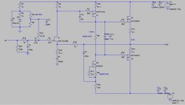
The star of this version is the ZVP2110G which Hugh and I decided was the best device available for this purpose.
Unfortunately the extra transconductance means that in my lash up the miller cap was needed for stability. I have not yet tried phase lead with this device, though it may also work.
Also, I had to make the device, which is an SMT item, fit in my current board which means the layout was messy. A proper PCB may have no such oscillation problems. Sounds great.
Attachments
using post1525 schematic.I do not understand your description above.
Bias current enters R4 (1k0), down through J1, across through R13 (1k0), across to output then down through Re (speaker), finally to Ground (0V0).
Let's assume that supply is +-25Vdc, bias current is 4mAdc, Re=6r0 and output offset is set to zero by adjusting the current unbalance at the output to -4mA, i.e. the output is acting as a -4mA source or 4mA sink.
The voltage at the bottom of R4 is 21V.
The voltage at the speaker output is 6r0 * [-4mA+4mA) = 0V0 precisely.
The voltage at the left end of the NFB upper leg is 4V0.
and J1 has (21-4) 17Vds.
Now, without adjusting the output offset pot, swap a 4ohm speaker for an 8ohm speaker. The new voltage at the speaker output -12mV offset. (this is confirmed by adding a second parallel speaker to the output). One would need to adjust the pot to bring back the output offset to 0V0.
Update.
today I checked output offset after warming up driving 8ohm.
+14mV to +15mV, a lot higher than previously measured.
added parallel 8ohm speaker. offset changes by just one or two tenths of a mV, whereas yesterday it moved -12mV from near 0v0. Odd behaviour. Today's temp is about 2Cdegrees lower than yesterday.
I am watching you copying my amplifier..ahahahahaha!
Your amplifier has stages... has VAS..also it has output... like mine.
Your amplifier uses supplies..... like mine
Your amplifier is connected to speakers...like mine
I am watching you!..... like you.
Carlos")
Your amplifier has stages... has VAS..also it has output... like mine.
Your amplifier uses supplies..... like mine
Your amplifier is connected to speakers...like mine
I am watching you!..... like you.
Carlos
Attachments

Without any intention of diverting this thread, my question is, what would be the effect of using 2SJ313 for the VAS and 2SK2013 for the CCS? What change of values to related passive devices? I am asking because I have these devices readily along with 2SK170BL and 2SJ162 and 2SK1058. Morever, I am right now stuck with a comp. which won't run any simulation software. Thanks.
Hey, just a thought. Now that the CCS is bootstrapped, it should have pretty even dissipation. Maybe it could be changed to a Jfet, for better performance?
Perhaps a GR grade 2SK170, with R18 being 1.8k, would give about 6-7V across it, for about 56mW of dissipation. There is plenty of room here to experiment with bootstrap values and voltages, to compromise between bootstrap and Jfet.
EDIT: I calculated this based on 8mA VAS current, but now I see in the schematic VAS current is 10mA.
I wish I had thought of this earlier.
- keantoken
Hi KT,
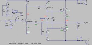
I modified one of my Fetzilla boards to the following:
Replace the input JFET with a 2SK117GR (lower gain).
Replace the VAS BJT (2SA1538) with a ZVP2110a.
Replace a few resistors to get the right bias current.
I am listening to it & surprisingly it sounds very good.
I don't have the DN2530 & the shipping charge is just too much for a small order. I will listen for a while before I replace R2 with a JFET (2SK117GR) CCS.
Cheers, Stanley
Attachments
Stan,
I didn't realise you still had a BJT in the VAS. You have been shooting yourself in the foot! The FET is light years ahead for this particular application.
I would switch to the 2SK170 for the input if you can. Higher gain in the input is essential for good bass with this amp, IMO.
Oh, and the CCS is also mandatory for good bass too, even a simple LED/BJT one will do.
Glad you like the sound.
Last edited:
Stan,
I didn't realise you still had a BJT in the VAS.
Glad you like the sound.
Hi Greg,
I have two Fetzilla boards, the first one is a rats-nest with the BJT VAS & I modified this version to try out the hybrid-CCS. The second one is a proper PCB with the ZVP2110a VAS and IRF610+LED as CCS. It is always good to have two boards to do incremental changes as my audio memory is short.
Cheers, Stanley
Last edited:
Without any intention of diverting this thread, my question is, what would be the effect of using 2SJ313 for the VAS and 2SK2013 for the CCS? What change of values to related passive devices? I am asking because I have these devices readily along with 2SK170BL and 2SJ162 and 2SK1058. Morever, I am right now stuck with a comp. which won't run any simulation software. Thanks.
Hi Sam,
The SJ313/K2013 are TO220 devices. I did a quick check & their spec are similar to IRF9610/610. You can try out the circuit as detailed in my post 1330.
If you like the sound, then order the proper FETs. The ZVP2110 does sound much better than the IRF9610.
Cheers, Stanley
Sam,
When people build kits, they invariably try to center it around their parts cache.
This amp has been developed around the semis chosen, and all passives support those choices. If you change the VAS, the heart of the amp, then degeneration, drain current, compensation and gate stopper are likely to require changing too. This of course is a substantial design modification, a bit like an engine transplant in an automobile.
I will be supplying both the input and VAS devices with my new pcb, and thus for the people on the group buy list this will not be a problem. If you do decide to use different devices, then you will need to re-engineer it, and while we will all be interested in your results, it will be a different amp and frankly, Greg and I are exhausted!!
I hope you understand, this has been a marathon and I'm looking forward to negotiating the logistics at this point,
Cheers,
Hugh
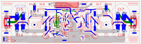
It's worth mentioning that Hugh has made a few independent changes to allow 36v rails and more power. I am happy with 25v rails and I prefer to run lower power and more bias current in the VAS and output as I can already play music louder than I care to.
Hugh's PCB is looking pretty nice and uses the ZVP2110G which has a perfect dissipation rating for this purpose and high transconductance.
Hugh's PCB is looking pretty nice and uses the ZVP2110G which has a perfect dissipation rating for this purpose and high transconductance.
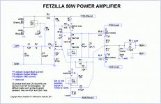
Hey Mike,
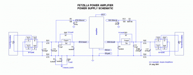
Here are the two circuits, unchanged from earlier!!
One is amp, the other, power supply. I've also included the pcb and the parts list. These will now be the OFFICIAL project documents as they incorporate corrections made courtesy Ken and George.
Paul actually drew it up for me, but it's the circuit I've designed the pcb for. Note that BOTH schematics are actually incorporated onto the ONE pcb. Two pcbs are required for a stereo pair, of course.
Ciao,
Hugh
Attachments
Last edited:
- Status
- This old topic is closed. If you want to reopen this topic, contact a moderator using the "Report Post" button.
- Home
- Amplifiers
- Solid State
- JFET input, MOSFET VAS, LATERAL output = Perfect!!