I dont think that the sound suffers by a lower OLG...
Well, this is dependant upon other factors.
I would agree with you if you have an extremely clean power supply, but in my experience whenever measures are taken to reduce PSU ( and other ) noise, the sound of the amp improves.
More FB, through Higher PSRR reduces PSU noise being expressed at the amp output so personally I would want to see extensive power supply filtering before I would be prepared to say that lower OLG does not decrease sound quality in some ways - even though it might improve it in other ways.
I will experiment with this when I have built my CLC PSUs.
mike
Hi Mikelm,
I have only built one channel.
Have you noticed that output offset varies with speaker load?
Open circuit is different from 8ohm and that is different from 4ohm.
This will also apply to headphones, particularly with the very wide range of HP impedances.
I cannot hear the 0.8mVac of hum with my speakers, not even a pair of 8ohms in parallel for an effective 4ohm loading and +6dB more hum.
I can easily hear that same 0.8mVac of hum through headphones. I will have to try rCRC instead of my rC supply.
The next channel will be built with output source resistors to see what effect they have that I am able to detect.
My small board layout does not suit modifying, but I knew that before I started.
the offset current flows through the NFB upper resistor and then through the speaker to ground. The output impedance of the output stage tries to bypass the speaker impedance. So yes high DC output impedance will force most of the offset current through the speakers or headphones.That offset changes with load probably only indicates that the amp has high DC output impedance, or that the supplies have high DC impedance.
- keantoken
It can still be trimmed out using the output offset adjuster, but that only holds low output offset, if one does not change the speaker/HP impedance.
the offset current flows through the NFB upper resistor and then through the speaker to ground. The output impedance of the output stage tries to bypass the speaker impedance.
Hi Andrew,
I do not understand your description above.
The NFB path and the speaker are normally in parallel.
my o/p impedance when I measured it 2 weeks ago was about 0.2 ohms
probably a bit less now
mike
Hey, just a thought. Now that the CCS is bootstrapped, it should have pretty even dissipation. Maybe it could be changed to a Jfet, for better performance?
Perhaps a GR grade 2SK170, with R18 being 1.8k, would give about 6-7V across it, for about 56mW of dissipation. There is plenty of room here to experiment with bootstrap values and voltages, to compromise between bootstrap and Jfet.
EDIT: I calculated this based on 8mA VAS current, but now I see in the schematic VAS current is 10mA.
I wish I had thought of this earlier.
- keantoken
Last edited:
KT,
Why would a jfet give better performance as a CCS than a DN2530 mosfet?
There are many circuits you come up with BTW where I think, Duh, why didn't I think of that? Not one of us can come up with everything new under the sun!!
Greg,
What is the measured value of the source rheostat beneath the mosfet? I would think around 100R?
Cheers,
Hugh
Erm, I dunno. The Jfet has lower capacitance.
To be honest, not having much experience with FETs of any kind, I don't really understand the mechanisms which make one better than another. My guess is that the one with higher Gm at the chosen current will have better self-regulation. However this effect is totally spoiled if Early effect (or it's FET equivalent) is bad.
The bootstrap takes care of the rails, so they aren't a concern for the Jfet. Here a good device must be chosen to prevent the MOSFET gate-source voltage distortions from entering the VAS via the CCS resistance.
Would it sound better? I don't know. I suspect in this case DC regulation is what we want in the CCS, capacitive effects seem to be taken care of. But I could be wrong.
D'oh, why didn't I think of ...
- keantoken
One question
Much earlier in the thread we switched to a simple resistor for setting o/p bias and now we're looking at an electrolytic across this to stabilise the voltage across this resistor . . . . I was wondering why we moved away from an amplified diode or diode chain + small variable R which I imagine would be quite good to give a defined voltage.
mike
Last edited:
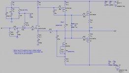
Hybrid CCS courtesy of Paul Bysouth
Sounds very very nice.
Hello
How does it sound compared to standard CCS and standard bootstap ?
Thank
Bye
Gaetan
Hello
How does it sound compared to standard CCS and standard bootstap ?
Thank
Bye
Gaetan
Hi Gaetan,
I amalgamates the surreal bootstrap vocal performance with the vastly superior bass performance of a conventional CCS quite nicely. I think it can be further improved by reducing the size of the bottom resistor.
Hugh,
I will check the value of that resistance tonight.
Hi Gaetan,
I amalgamates the surreal bootstrap vocal performance with the vastly superior bass performance of a conventional CCS quite nicely. I think it can be further improved by reducing the size of the bottom resistor.
Hugh,
I will check the value of that resistance tonight.
Hello
And the soundstage ?
Thank
Bye
Gaetan
Thanks Greg!
Mike,
On the pcb I'm having made there is indeed a three diode string, with a 200R variable pot, to set the output bias. This means that the adjustment range is nicely limited, and different VAS currents can be trialled. There is even a 4.7V zener across the bias generator to limit quiescent to no more than about 2.5A in case of 'accidents'.
The Fetzilla board incorporates many options for stability. There is space for a miller cap, a phase lead cap, and a shunt cap across the series 1K fb resistor to tidy up phase shift at high frequencies. None have to be used; but the option is conveniently there. This gives tolerance for a wide variety of speaker loads, including electrostatics. It also permits tweaking for those so inclined.
Cheers,
Hugh
SWF, Bootstrap performance will be increased by increasing the bottom resistor. However this will give less Vds for the CCS. Vds dramatically impacts CCS performance in this case. Higher is better. So there may be a tradeoff between bootstrap performance and CCS performance. Usually I go for no less than 5V.
- keantoken
- keantoken
This is the most perfect amplifier I have spiced.
It is simple but yet very, very good.
- JFET input with minimal offset problems.
- MOSFET VAS for speed and gain
- LATERAL output for be a light load to VAS
When CLass AB operation, 350mA bias, it shows only
THD 0.00018% at 1 Watt
And there is almost no increase of THD at 25 Watt output
Enjoy!!")
Mr. lineup
Is you can create a simulation of this mosfet amplifier with IRFP250 (see Figure 1), since I have a problem with the output transistor IRFP250 burn?
thanks
Attachments
- Status
- This old topic is closed. If you want to reopen this topic, contact a moderator using the "Report Post" button.
- Home
- Amplifiers
- Solid State
- JFET input, MOSFET VAS, LATERAL output = Perfect!!