I believe the syntax is explained below the netlist in the stuff you linked to.
Another thing is to be aware that the netlist, which is the model the sim uses and is just a bunch of text describing the part, is something else than the schematic symbol. Strictly speaking you don't need a chematic symbol - it's just for your convenience. You could draw a schematic symbol as a block with some pins with the same name as the connections on the .subckt line in the netlist and wire it up and it would work.
If your model netlist says: .subckt mymodel Vin Vout Bias Vcc Vee that defines to the sim a part that is called mymodel an that has pins with the given name, in that order.
Then below the .subckt line you get the actual model description, like the 'circuit' internal to the model that the sim uses for its calculations.
You see things like Rin Vin 0 10k that defines a 10k resistor between pin Vin and ground. You can also use R44 Vcc Bias 2k2 as a resistor from Vcc to Bias etc.
Makes sense?
Jan
Thanks for your reply. I have no issue understanding the simple resistor with two nodes and value. I think I know enough to write the whole circuit by netlist file at this point. It does not help me a bit to even understand the simple 3 line subcircuit file shown below.I just copy out the example in the link:
.subckt GainBlock AMP_IN AMP_OUT PARAMS: gain=10 Rin_value=50
Rin AMP_IN 0 {Rin_value}
Eamp 1 0 AMP_IN 0 {gain}
.param Rout_value=100
Rout 1 AMP_OUT {Rout_value}
.ends GainBlock
1) Eamp is a voltage control voltage source. What is the syntax? From
Eamp 1 0 AMP_IN 0 {gain},
the syntax is (Eamp, A, B, C, D {#value})
a) What is the definition of Eamp? Is it another subcircuit with parameters A, B , C, D and the #value?
b)What is A, B ,C, D stand for? The only one I can guess is C=Amp_IN node. That B and D is grounded.
2) The description said Rout defined the output impedance. The output impedance of Eamp has to be zero as it's a voltage source. The Rout HAS to be in series with the output of Eamp before driving AMP_OUT. How does the following describe Rout is in series with the output of Eamp connecting to AMP_OUT;
Rout 1 AMP_OUT {Rout_value}
These are just two lines that I have no idea what to make of. This is a lot more than simple (R A B #value) to describe a resistor where A an B are just two nodes the resistor connecting to. Or (Q C B E npn) to describe a transistor with the nodes connecting to C,B and E that found in the simple netlist file.
3) Also, Why the first line only define "PARAMS: gain=10 Rin_value=50" why not puttingRout_value=100 in the first line and has to use another line.param Rout_value=100?
These are the stuffs you can't learn by reading the normal netlist files.
Last edited:
I basically don't know the syntax of the subcircuit. I know the basic netlist file where (R node1 node2 value). But I have no idea how the subcircuit is defined. I high lighted a few below in red and questions followed in blue.
This is like FPGA programming where you call a subroutine like a Flip Flop etc, but you have to define the parameters to be exchange and link to the subroutine. I can see it started with top level as subcircuit MAX44263, then call subcircuit X_1 and X_2, which then call OY69........ That's where I get totally lost!!!
If you can point me to the syntax of this, I'll be really appreciated. I have been searching up and down for this, all the articles seems to talk about the basic netlist files.
*** MACROMODEL FOR MAX44263 ***
* ----------------------------
* Revision 1. 08/2012
* ----------------------------
*******************************************
.subckt MAX44263 OUTA INA- INA+ VSS INB+ INB- OUTB VDD
I thought the normal single opamp defined as +IN,-IN,Vcc, Vee, OUT.
X_1 OUTA VSS INA+ INA- VDD OY69
X_2 OUTB VSS INB+ INB- VDD OY69
What is this? X_1 and X_2 are subcircuits defined for MAX44263?
.ends
*******************************************
.subckt OY69 IN+ VSS IN- OUT VDD
X_1 OUT VSS IN+ IN- VDD opamp
.ends
*******************************************
.SUBCKT opamp 201 18 17 15 10
***************
*INPUT STAGE
VS1 10 11 0V
GBIAS 11 12 304 100 179.25U
What is G? Generator? What is the definition of all the nodes?
M1 13 16 12 11 MOSFET
M2 14 15 12 11 MOSFET
DBIAS 18 12 DY
EOS 17 16 VALUE={-10u+V(10)*(-9u)}
What is E and what are the nodes?
RD1 13 18 1K
What is RD? Is the LTSpice just read the first letter R and determine it's a resistor with two nodes connecting to node 13 and 18 and with value 1K?
RD2 14 18 1K
C1 13 14 2P
CIN1 16 100 10P
CIN2 15 100 10P
DIN1 16 11 DA
DIN2 18 16 DA
DIN3 15 11 DA
DIN4 18 15 DA
FSUP 18 10 VS1 1
E103 103 18 10 18 1
**************
*INPUT BIAS CURRENT
IBIAS1 18 17 -1P
IBIAS2 18 15 4.98P
GBIAS1 17 18 10 18 1p
GBIAS2 15 18 10 18 1p
RID 15 16 1000G
**************
**************************************************
*GAIN STAGE
GA 25 100 14 13 2.2M
RO1 25 100 2.95k
GB 26 100 25 100 110M
RO2 26 100 1K
EF 27 100 26 100 1
CC 25 27 70P
EF2 29 100 28 100 1
GC 100 28 26 100 142.16M
RO3 28 100 2.7K
CC2 25 29 50p
RO4 28 30 20
GCMPS 100 25 40 100 393.5U
**************
*CURRENT LIMIT
DP3 26 38 DY
EP3 38 100 10 18 185M
DP4 39 26 DY
EP4 100 39 10 18 185M
**************
*INTERNAL GND
EG1 100 18 10 18 0.5
**************
*VOLTAGE LIMITING
VS2 30 31 0V
*****
DP1 30 32 DY
HP1 34 32 VS2 17.72
EP1 34 36 10 18 0.5
VOFF1 100 36 12M
*****
DP2 33 30 DY
HP2 35 33 VS2 14.43
EP2 37 35 10 18 0.5
VOFF2 37 100 12.8M
***************
*CMRR
RRR 40 100 1
GCMR 40 100 12 18 400u
GPSR 100 40 10 18 300u
***************
*SUPPLY CURRENT
ISUP 10 18 -600u
GSUP 10 18 10 18 -40u
***************
*FOR SHUTDOWN
MEN1 171 172 31 10 MOSFETP
MEN2 171 173 31 18 MOSFETN
EEN3 170 172 304 100 10
EEN4 173 170 304 100 10
RSHUNT 170 171 10MEG
VIS5 171 400 0V
R171 171 18 100k
D401 400 401 DY
D402 402 400 DY
D403 201 401 DY
D404 402 201 DY
I400 401 402 50m
Foo 400 18 VIS5 -0.88
********************************
RSH 103 18 500MEG
ISH 18 103 10NA
DSH 103 10 DY
CSH 103 18 10P
**************
EEN2 300 100 103 18 1
REN 300 301 10K
VEN 301 302 0V
EHYST 303 302 POLY(2) 10 18 304 100 0 0 0 0 0.4
EEN1 303 100 10 100 0.7
**************
FEN1 100 304 VEN 12
CEN 304 100 1P
DEN1 100 304 DY
DEN2 304 305 DY
VLIM1 305 100 1V
**************************************************
.MODEL DA D(IS=100E-14 RS=0.5k)
.MODEL MOSFET PMOS(VTO=-0.2 KP=29.3E-3 KF=26E-25 AF=0.8)
.MODEL DX D(IS=100E-14)
.MODEL DY D(IS=100E-14 N=10M)
.MODEL MOSFETP PMOS(VTO=-5.0 KP=88E-3 GAMMA=0.01)
.MODEL MOSFETN NMOS(VTO=5 KP=88E-3 GAMMA=0.01)
**************************************************
.ENDS
thanks
Last edited:
I spent a lot of time reading .subcircuit and circuit elements and I solve the problem. The problem is MAX44263 is a dual opamp with different pinout definition. To using Opamp2, you need to modify the .txt file:
1) Opamp2 pins sequence is IN+ IN- VDD VSS OUT but
2) Maxim is:
.subckt MAX44263 OUTA INA- INA+ VSS INB+ INB- OUTB VDD(1)
X_1 OUTA VSS INA+ INA- VDD OY69
X_2 OUTB VSS INB+ INB- VDD OY69
.ends
.subckt OY69 IN+ VSS IN- OUT VDD
X_1 OUT VSS IN+ IN- VDD opamp (2)
.ends
.SUBCKT opamp 201 18 17 15 10 (3)
1) Look at (2) and (3), we know
OUT is node 201
VSS is node 18
IN+ is node 17
IN- is node 15
VDD is node 10
2) Compare to(1), we change(1) to .subckt MAX44263 OUTA 17 15 10 18 201
And delete all the rest, just keep (3).
I bypass all the calling of subcircuits and follow the files from Analog devices that called out the internal nodes straight to the main subcircuit.
I also attach the copy of the description of the elements and some relevant information if people like to get into the netlist and subcircuits.
The Yahoo LTSpice group is by far the most useful place to learn LTSpice, there are a few people that really know what they are doing.
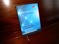
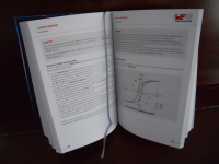
It has arrived.
Received my copy of 'The LTSPICE IV Simulator' today.
Over 700 pages, hardback, beautifully bound and all the pages are almost photographic gloss quality. It looks like it will prove to be worth its weight as they say.
Received my copy of 'The LTSPICE IV Simulator' today.
Over 700 pages, hardback, beautifully bound and all the pages are almost photographic gloss quality. It looks like it will prove to be worth its weight as they say.
Attachments
A slow Sunday?!6 weeks since the last LTSpice engine update. I hope all is well at Linear Tech
Looks like the last change to the basic executable files was back in January. Run the "Sync Release", then check the "Changelog.txt" file. There have been recent changes to models and symbols but they've stopped incrementing the Version designation every time one of those support files changes.6 weeks since the last LTSpice engine update. I hope all is well at Linear Tech
Dale
Hi Guys,
Today for the first time ever I successfully added some models to the LT spice Library - Thx for the advice here for that.
However, I am really struggling to get this sub circuit into a regular N channel mosfet symbol.
I tried using the op amp subckt example shown here without success - would appreciate some step by step idiots guidance")
*ZETEX ZVN4424G Spice Model v1.2 Last Revised 20/3/01
*
.SUBCKT ZVN4424G 3 4 5
*------connections-------D-G-S
M1 6 2 8 8 N4424AM
M2 6 2 8 8 N4424AMS
RG 4 2 9
RD 3 6 3.6
RS 8 5 0.15
RL 3 5 240E6
C1 2 8 137E-12
C2 2 3 15E-12
C3 15 14 385E-12
C4 16 8 220E-12
D1 5 3 N4424AD
S1 2 15 13 14 SMOD1
S2 13 15 14 13 SMOD1
S3 16 13 13 8 SMOD2
S4 16 2 8 13 SMOD2
Egs2 13 8 2 8 1
Eds1 14 8 3 8 1
.MODEL N4424AM NMOS VTO=1.3 IS=1E-15 KP=0.85
+CBD=66.2E-12 PB=1
.MODEL N4424AMS NMOS VTO=.86 IS=1E-15 KP=0.0085
+CBD=.66E-12 PB=1
.MODEL N4424AD D IS=5.516E-13 RS=.2084 N=1.0078
.MODEL SMOD1 VSWITCH RON=.001 ROFF=100 VON=1.5 VOFF=1
.MODEL SMOD2 VSWITCH RON=.001 ROFF=100 VON=-0.5 VOFF=-2.5
.ENDS ZVN4424G
*
*$
*
Today for the first time ever I successfully added some models to the LT spice Library - Thx for the advice here for that.
However, I am really struggling to get this sub circuit into a regular N channel mosfet symbol.
I tried using the op amp subckt example shown here without success - would appreciate some step by step idiots guidance
*ZETEX ZVN4424G Spice Model v1.2 Last Revised 20/3/01
*
.SUBCKT ZVN4424G 3 4 5
*------connections-------D-G-S
M1 6 2 8 8 N4424AM
M2 6 2 8 8 N4424AMS
RG 4 2 9
RD 3 6 3.6
RS 8 5 0.15
RL 3 5 240E6
C1 2 8 137E-12
C2 2 3 15E-12
C3 15 14 385E-12
C4 16 8 220E-12
D1 5 3 N4424AD
S1 2 15 13 14 SMOD1
S2 13 15 14 13 SMOD1
S3 16 13 13 8 SMOD2
S4 16 2 8 13 SMOD2
Egs2 13 8 2 8 1
Eds1 14 8 3 8 1
.MODEL N4424AM NMOS VTO=1.3 IS=1E-15 KP=0.85
+CBD=66.2E-12 PB=1
.MODEL N4424AMS NMOS VTO=.86 IS=1E-15 KP=0.0085
+CBD=.66E-12 PB=1
.MODEL N4424AD D IS=5.516E-13 RS=.2084 N=1.0078
.MODEL SMOD1 VSWITCH RON=.001 ROFF=100 VON=1.5 VOFF=1
.MODEL SMOD2 VSWITCH RON=.001 ROFF=100 VON=-0.5 VOFF=-2.5
.ENDS ZVN4424G
*
*$
*
Received my copy of 'The LTSPICE IV Simulator' today.
Over 700 pages, hardback, beautifully bound and all the pages are almost photographic gloss quality. It looks like it will prove to be worth its weight as they say.
I'm going to sell it from the Linear Audio website. Probably a better deal
And for those hesitating, here's Bob Cordell's review.
Jan
Last edited:
I look forward to buying this book from your site. Vol 9, and 8 are heading my way.I'm going to sell it from the Linear Audio website. Probably a better deal
And for those hesitating, here's Bob Cordell's review.
Jan
I'm going to sell it from the Linear Audio website. Probably a better deal
And for those hesitating, here's Bob Cordell's review.
Jan
Nice one

Just read Bobs write up and review, it looks bang on the money to me
For all those interested in LT, this is money well spent imo.
Nice one
Just read Bobs write up and review, it looks bang on the money to me
For all those interested in LT, this is money well spent imo.
Mine arrived last week, ordered after reading Bob's review. Well worth the money (£25) and as a newcomer to LTSpice, it's proving very useful.
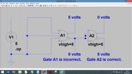
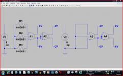
Can anyone explain what I'm missing here.
I have been thinking of adding a section on using logic devices buthave discovered a fundamental problem... which no doubt is something I am missing.
Here we have two AND gates selected from LT's library. Rather thoughtfully these include the inverted or NAND output as well.
The problem is evident when looking at the two versions here. To get the correct logic function on gate A1 needs the inclusion of the series input resistors. Even making these 0.00001 ohms works. Make them a link and the gates two outputs flip states.
The asc file is attached if anyone wants to play with it. Just link the resistors out and see how the function of A1 reverses.
What am I doing wrong
Attachments
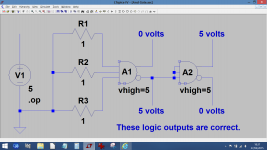
The blue text is just added comment. the vhigh=5 applies to just the symbol telling the gate to operate as if it were on a 5 volt supply.
If you hover the cursor over the lines you see the voltages.
Try this, the two circuits side by side. The blue text is now LT generated when the file is run and shows the voltage as LT calculates them.
If you hover the cursor over the lines you see the voltages.
Try this, the two circuits side by side. The blue text is now LT generated when the file is run and shows the voltage as LT calculates them.
Attachments
dear Mooly,
for digital/logic part i use this library
http://valvolodin.narod.ru/soft/extra.rar
models
for digital/logic part i use this library
http://valvolodin.narod.ru/soft/extra.rar
models
Hi Mooly,
FIRST: Many-many THANKS from all beginners for his work on tutorial !
I am trying to make my first model, this Chinese amplifier kit L7:
2pcs Class AB MOSFET L7 Audio Power Amplifier Kit Mono 300 350W | eBay
I rebuilt circuit from PCB, and try simulate distortion, but result is very very bad, unreal bad.
I do not see where my mistake in model.
If possible - help solve problem. Thanks for any help in advance. Alex.
Attachments
- Home
- Design & Build
- Software Tools
- Installing and using LTspice IV (now including LTXVII), From beginner to advanced