The passive filter solves the droop beautifully but I have found it detrimental to the bass. Perhaps that's why there's a correction in the filter but it's not working very well.
But now I think the DAC has potential I reckon the active I/V is worth a punt. A few questions though:-
With active I/V do you still need 4, 8 dacs in parallel?
Why are you using 6V? I want to keep using the USB voltage or boost it to 6V but the noise that may introduce may warrant keeping it at the ~ 5V line. Any changes to your circuit to do that? Also the datasheet says 5.5v max!
What is BREF?
What is the difference between the upper & lower circuits, is it just to support the LED? What does the LED represent?
Last edited:
Could you please share kicad files or similar of the new three stack pcb's?
I'm very curious to build this interesting dac.
Hi Yo - there are a few errors on the existing DAC PCB so you'd need more than just the kicad files (actually the PCBs were done on easyEDA, not kicad as my gf prefers that). We have a new DAC PCB coming along very soon (hopefully it'll come back from the factory this week) and that fixes up some issues on that board. The filter and buffer PCBs don't have any significant errors on them.
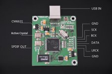
Given that blogs are currently unavailable here, I've shared info on this DAC over on Hackaday, here is the URL : Audiophile-sounding DAC for almost no money | Hackaday.io
With active I/V do you still need 4, 8 dacs in parallel?
No, you can do active I/V with any number of DAC chips, starting at 1.
Why are you using 6V?
I'd like to get the maximum amount of output current from the minimum number of chips. Also the higher voltage is necessary to obtain 1VRMS output swing. 6V is the highest safe voltage, so 6V it is.
I want to keep using the USB voltage or boost it to 6V but the noise that may introduce may warrant keeping it at the ~ 5V line. Any changes to your circuit to do that? Also the datasheet says 5.5v max!
I found running DACs on the USB supply direct from the PC resulted in some feed-through from the PC itself. Even when I used an LC filter.
If you want to run at 5V you'll need to accept a lower output voltage, say 0.7VRMS.
What is BREF?
A reference voltage for the bases of the I/V transistors. One reference is shared between L and R channels. The LED is being used as a voltage reference to create BREF.
BREF is now making sense - I guess you're using the LED as a 2v level?
The TDA1387 rates the chip @ 5.5V max, but i assume you've tested it no problem.
is there any benefit in using 4 DAC's over 1 with active I/V?
I had a look at your schematics, I'm contemplating whether to have the active I/V made on some cheap prototypes or to go the whole hog and do the lot rather than trying to breadboard your I/V and a 6V boost.")
The TDA1387 rates the chip @ 5.5V max, but i assume you've tested it no problem.
is there any benefit in using 4 DAC's over 1 with active I/V?
I had a look at your schematics, I'm contemplating whether to have the active I/V made on some cheap prototypes or to go the whole hog and do the lot rather than trying to breadboard your I/V and a 6V boost.

Looking at this to convert USB to I2S.
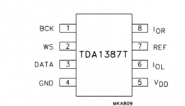
The TDA1387 has BCK, WS and DATA
WS = SCK?
No, WS = LRCK.
Not sure what SCK is.
Ok, it's starting to look like a new PCB to do the lot. Why do you use a second chip with inverted data?
Its my way of keeping the power supply draw constant. Otherwise the PSU gets modulated by the digital data, something undesirable.
Which USB 2 I2S do you use? I see the elderly DP106 (aka CM106 with I2S) used on the L1387 is Isocronous. I'd prefer an async chip.
If I don't care about jitter, then CM108. When I do, then CM6631A.
I think SCK means 'system clock' or another name for it would be 'master clock'. This is normally something like 256fs and its needed by some DACs that do high-order oversampling (S-D ones, in general). TDA1387 has no need of such a high clock frequency.
'Active filter' ? I don't have one.
Last edited:
Why do you use a second chip with inverted data?
Its my way of keeping the power supply draw constant. Otherwise the PSU gets modulated by the digital data, something undesirable.
Also: I use a second tda1387 with inverted data so I can have balanced output. I.e., one dac chip outputs the positive right and left channels, and the other chip outputs the negative right and left channels.
Take a look at this thread if you haven't already. There's a lot of general tda1387 info there that you might find useful if you're interested in this chip.
The passive filter solves the droop beautifully but I have found it detrimental to the bass. Perhaps that's why there's a correction in the filter but it's not working very well.
It's because correcting a high frequency roll off will give the impression that there is less bass. That is pretty much how we hear; a high frequency roll off might not necessarily come off as lacking in treble, but sound like fullness in bass. And a more neutral response will sound bass light.
Cool, I'm ordering one then.
Now all I need is for abraxalito to explain what components need to change in his filter for 1 DAC, and how the LED works as a reference (why not use a resistor + zener)?
Now all I need is for abraxalito to explain what components need to change in his filter for 1 DAC, and how the LED works as a reference (why not use a resistor + zener)?
Attachments
It's because correcting a high frequency roll off will give the impression that there is less bass. That is pretty much how we hear; a high frequency roll off might not necessarily come off as lacking in treble, but sound like fullness in bass. And a more neutral response will sound bass light.
It's not just less, it's gone quasi as if there's some cancellation going on. It's not right, put it that way.
No matter, going for "active" I/V.
Matt how come you didn't use abraxalito's transistor I/V conversion in your design?
Last edited:
My intention is to use the attached board footprint then mount a second PCB containing;
1. a 12V boost and a 6V LDO using smd components. (minimal noise)
2. a single TDA1387
3. abraxalito's filter using smd components
Let me know if anything's missing. I'll post the Kicad files once I'm done.
1. a 12V boost and a 6V LDO using smd components. (minimal noise)
2. a single TDA1387
3. abraxalito's filter using smd components
Let me know if anything's missing. I'll post the Kicad files once I'm done.
Attachments
Last edited:
Matt how come you didn't use abraxalito's transistor I/V conversion in your design?
Which design are you talking about?
In my "front end" design (the original topic of the thread I linked above), the idea was to create a basic building block for tda1387-based designs. By default it had passive I/V, simply because that's trivial to implement. But the user could easily switch to "current out" mode via jumper settings, and have the raw DAC output, which could in turn to go whatever "back end" circuits one wanted to test (e.g. filters, buffers, I/V stages, etc). I also figured some people might find passive I/V adequate.
Not long after creating the "front end" I switched gears to making DAC HATs for the Raspberry Pi. In those designs I did use Abraxalito's common-base transistor I/V.
Now all I need is for abraxalito to explain what components need to change in his filter for 1 DAC, and how the LED works as a reference (why not use a resistor + zener)?
I'll put up a new version of the schematic on the dedicated lingDAC thread I shall be opening shortly. The LED voltage is below any zener diode I've come across - have you ever seen a zener diode with a breakdown voltage below 2V? If so do send me a link.
- Status
- This old topic is closed. If you want to reopen this topic, contact a moderator using the "Report Post" button.
- Home
- Source & Line
- Digital Line Level
- Impressions: USB DAC: TDA1387 NOS vs PCM5102A Delta-Sigma