Don't be so fast in your judgement, PMA.
Your test does not say anything. You need to test your amps with different transformer sizes and transformer types.
I would recommend trying a large Rcore for ex. and maybe even try using two transformers - one for each channel.
Could it be that some amps are more affected by transformer size than others?
A few years back you would not have said that you could hear that a 10 cm wire can sound different from another 10cm wire.
Sigurd
PMA said:
Superstition.
jgedde said:Syn08, That board sure is handsome. Did you etch it yourself? How did you do the solder plating and have it so smooth and level?
John
I don't etch my own boards, but order from (shipping next day):
- www.apcircuits.com (Canada) for small sizes (2 pcs. minimum order).
- www.barebonespcb.com (US) for large sizes (5 pcs. minumum order).
Shipping from US is outrageous ($75 FeDex plus 13% Canadian taxes), while apcircuits costs are much higher. I built a spreadsheet with cost/sizes and found the threshold (depending on size and number of boards). For cost reasons, I don't do solder masks and silkscreens.
analog_sa said:Cute and probably not bad sounding. Power transformer is about 20 times smaller than what i useJung regs or not this is quite audible.
The whole thing draws 80mA from the +18V supply and 40mA from the -18V supply. Filtering is 10,000uF per rail (2 x 4,700uF). If anybody has a good reason why a large power transformer would be required, speak up. "sounds better" is not good enough for me.
Re: Re: Hps 2.0
The huge red caps are SuperCap polypropylene C6 in the schematic. Sorry, they are 10uF/250V not 22uF. 22uF is an overkill.
Adjustable gain could be done by just another DIP switch, will think about if there will be another release (little reason so far).
I don't think it's reasonable to adjust the input impedance externally. It could be done via relays and sone decoding logic, but price and complexity could be prohibitive. BTW, I think this design pretty much closes the discussion about good quality (and wisely used) reed relays as not good for the ultimate performance. Just another legend...
Gains are (as in the previous design) 46dB for MM and 64dB for MM. Haven't looked at the overload margins but the opamp swings are the limiting factor and the supplies are +/-18V. Due to the FB loop, the input gain stage output swing is very small.
Sigurd Ruschkow said:Good to see that you decided to improve the design!
The huge red caps in the upper right corner and in the middle, what types are those?
Ideas for improvement could be to have adjustable gain, and adjustable input resistors for MC cartridges (although doing this manually might be the best solution).
BTW,
what gains do you have,
and what are the overload margins?
Sigurd
The huge red caps are SuperCap polypropylene C6 in the schematic. Sorry, they are 10uF/250V not 22uF. 22uF is an overkill.
Adjustable gain could be done by just another DIP switch, will think about if there will be another release (little reason so far).
I don't think it's reasonable to adjust the input impedance externally. It could be done via relays and sone decoding logic, but price and complexity could be prohibitive. BTW, I think this design pretty much closes the discussion about good quality (and wisely used) reed relays as not good for the ultimate performance. Just another legend...
Gains are (as in the previous design) 46dB for MM and 64dB for MM. Haven't looked at the overload margins but the opamp swings are the limiting factor and the supplies are +/-18V. Due to the FB loop, the input gain stage output swing is very small.
scott wurcer said:
BTW, did you really have no use for the little bit of distortion removal via the 50pf extra cap on the first amp? It's possible there is little or no difference in this circuit.
Scott,
If you are looking closely at the signal board you'll notice a couple of unused holes close to each opamp. These are provisions for the distortion cancelling caps. I may install them one day but, to my experience, the impact here will be negligible.
BTW, for noise reasons, AD797 is really required only in the input stage. For the rest, I was unable to find any measurable difference to other good quality opamps (tried lots, from OPA211 to LME49710). I liked though more AD797 in the second stage and LME49710 in the output stage.
And another BTW, the power supply uses LT1115 and I got 7nV/rtHz output noise.
Sigurd Ruschkow said:Don't be so fast in your judgement, PMA.
Your test does not say anything. You need to test your amps with different transformer sizes and transformer types.
Especially present audiophiles were perplexed by the test result, considering price, power input (not output), capacitors and weight of the competition device.
PMA said:
Especially present audiophiles were perplexed by the test result, considering price, power input (not output), capacitors and weight of the competition device.
At the risk of repeating myself comparing different topologies is completely meaningless with respect to the transformer effect. Glad that your amp managed to perplex. Imagine how much further the perplexion would have gone with a proper PS
But audio is rarely a match terminated affair (i.e. you have minimal control over your source impedance), noise figure is more useful maybe if you are using transformers.
If you mean taking an audio band RMS meter and increasing the source until you get +3dB, that is a good way to eliminate gain and frequency response from the measurement. But the presense of 1/f noise can give errors, especially with the low boost of RIAA.
If you mean taking an audio band RMS meter and increasing the source until you get +3dB, that is a good way to eliminate gain and frequency response from the measurement. But the presense of 1/f noise can give errors, especially with the low boost of RIAA.
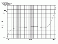
Finally got some time to precisely measure the RIAA errors. The attached is the difference between the measured frequency response and the ideal RIAA response, synthesized by the pole-zero method (two poles at 50Hz and 2.12314KHz and one zero at 500Hz; the mythical f4 zero at 50KHz was not included here). Both the measurements and the synthesis were performed in a HP3562A DSA.
The graph shows clearly that the +/-0.1dB target (20Hz-20KHz) was reached. The shape of the curve is very close to the Hagerman results http://www.hagtech.com/pdf/riaa.pdf in fig. 7
Now, certainly, +/-0.1dB is and absolute overkill. Assuming the decrease in intensity of a spherical wave as it propagates outward in air as an inverse square law, and a listener at 10ft., 0.1dB is equivalent to the variation you would get by moving the listener by plus or minus 3/8 of an inch, off axis. Anybody willing to set up a test and report back the audibility of such and error?
Anyway, for any practical purposes, +/-0.2dB should be more than enough.
Attachments
I agree on the tendency for some to obsess on RIAA accuracy. My big divergence from most is this. How often do you change cartridges? Me rarely, so I solder everything in permanently, by this I mean termination R&C, and all connectors too.
If you think about it a new cartridge means a set up (draging out the Dennesen Protractor or whatever). The time spent soldering new termination components is small change.
If you think about it a new cartridge means a set up (draging out the Dennesen Protractor or whatever). The time spent soldering new termination components is small change.
john curl said:With this kind of phono stage, a very good way of measuring noise is NOISE FIGURE. Yes, just find an equivalent resistor that, when placed on the input, gives a 3dB noise figure. Works for me, and it takes in EQ, and everything.
NF could be easy to determined this way, but ultimately it's the S/N that really matters. You can choose a higher Rg to reduce NF to almost zero (because we are talking here about JFETs, having current noise essentially zero). In this particular case, the Rg noise would be the major noise source and if you are looking at the NF formula, this would render a NF very close to zero. You just got an example of a very low NF but a very low S/N as well. Which means that a low NF number tells by itself squat about "low noise".
Now, of course, one can use a standard Rg and do a meaningful comparation between various systems or implementations noise. However, as Scott also mentioned, audio is not an impedance matching game so, depending on application, chosing 50ohm may be as good (or meaningful) as chosing 10ohm or 1Kohm. I have never seen any attempt to standardize Rg in audio for noise purposes...
So I would stick to equivalent input noise or S/N rather than on NF.
Unfortunately, you just don't get it. The NF measurement can be used effectively to rate the overall noise of an input stage. It works very well in practice, IF you have a low noise design, and especially with a jfet or tube input, so that current noise is completely out of the equation. However, if I took Scott Wurcer's AD797, I could get good results also.
john curl said:Unfortunately, you just don't get it. The NF measurement can be used effectively to rate the overall noise of an input stage. It works very well in practice, IF you have a low noise design, and especially with a jfet or tube input, so that current noise is completely out of the equation. However, if I took Scott Wurcer's AD797, I could get good results also.
Unfortunately John, but not unexpected, you don't get it. I'm suspecting you did not even read my comment but, as usual, you just posted a short dismissal. Do yourself (and your reputation as "low noise specialist") a favour and at least read again the 2SK170 datasheet. You'll notice that the NF is specified at a certain Rg. Without that value, comparing NF's is as stupid as comparing apples and oranges. Now if I'm telling you that my HPS has a NF of 2.1dB, how would this help anybody compare with other implementations?
Don't bother to answer before finishing your homework.
Surely it s jus t easie r to quite equivalent input nois e voltage and current. That way, the real world performance can be determined quickly for any input source.
Natsemi had a very nice app note on this (there was a link somewhere on this forum) where they cautioned about using NF precisely because the source needs to be clearly defined. Great for RF (usually 50 Ohms), but maybe a les s practical for situations where the source is not standardized.
Natsemi had a very nice app note on this (there was a link somewhere on this forum) where they cautioned about using NF precisely because the source needs to be clearly defined. Great for RF (usually 50 Ohms), but maybe a les s practical for situations where the source is not standardized.
HPS 3.0
Full concept schematic (shown here with THS4031, a good alternative here to AD797, SMD though). Whatever very low noise opamp will work here instead, but has to have pretty high output current (around 100mA) to drive the feedback network under overload conditions.
High voltage opamps are used for the rest, to provide a large headroom.
Some minor changes may eventually occur. The PCB schematic has onboard provisions for input impedance switching and gain control via DIP switches.
Key performance:
0.25nV/rtHz with selected (for noise) and matched JFETs.
0.30nV/rtHz with average JFETs Idss=11 +/- 0.5mA
83dB SNR unweighted, 0.5mV input signal, 64dB gain.
>92dB SNR RIAA, 0.5mV input signal, 64dB gain.
28dB headroom (+/-24V supplies).
+/-0.1dB RIAA match
End to end DC coupling with servo (<1mV DC output); output cap is optional.
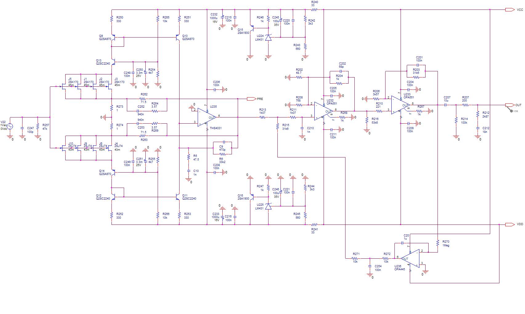
Re: HPS 3.0
You mentioned simulations. I have found sims to be accurate regarding noise analysis.
If you simulate your design with your JFET models, how much discrepancy do you get between real world measurements and simulations?
And how does your JFET models look like graphically noisewise?
Sigurd
QUOTE]Originally posted by syn08
Full concept schematic (shown here with THS4031, a good alternative here to AD797, SMD though). Whatever very low noise opamp will work here instead, but has to have pretty high output current (around 100mA) to drive the feedback network under overload conditions.
High voltage opamps are used for the rest, to provide a large headroom.
Some minor changes may eventually occur. The PCB schematic has onboard provisions for input impedance switching and gain control via DIP switches.
Key performance:
0.25nV/rtHz with selected (for noise) and matched JFETs.
0.30nV/rtHz with average JFETs Idss=11 +/- 0.5mA
83dB SNR unweighted, 0.5mV input signal, 64dB gain.
>92dB SNR RIAA, 0.5mV input signal, 64dB gain.
28dB headroom (+/-24V supplies).
+/-0.1dB RIAA match
End to end DC coupling with servo (<1mV DC output); output cap is optional.
[/QUOTE]
- Status
- This old topic is closed. If you want to reopen this topic, contact a moderator using the "Report Post" button.
- Home
- Source & Line
- Analogue Source
- GPP - Great Phono Preamp