Cool!Godfrey - I made some changes according to your suggestions. I'm going to leave the 1uF/100V capacitors where they are... The temperature near the MOSFEST will be high and it's better if these caps are slightly positioned away from the transistors.
")
BTW the reason I suggested moving the zobel is to open up the red current path, otherwise there's only the green. Better than nothing, though.
Attachments
NagysAudio, you manage to build a real Goldmund clone.
Why do not copy widely the original Goldmund PCB (routing, ground plane, etc...) ?
This would be easier and give more waranty of the final result.
NB : I think you have the possibility de take pictures of all the details on Goldmund 9 or 3....
Thanks
Why do not copy widely the original Goldmund PCB (routing, ground plane, etc...) ?
This would be easier and give more waranty of the final result.
NB : I think you have the possibility de take pictures of all the details on Goldmund 9 or 3....
Thanks
Luke - I can ask you the same question: Why all the fuss over these resistors?
I will also repeat this for the 3rd time: Individuals who would like to use the source resistors can install them between the two MOSFETS' mounting bolts. This is actually the easiest way to install them if using TO3 transistors and the proper way. No changes need to be made to the PCB. Therefore, I obviously cannot take these requests.
1.) Cut the resistor's leads to correct length.
2.) Solder a ring terminal on each end of the resistor.
3.) Take the nuts off from the bottom of the PCB, the ones that hold the MOSFET in place.
4.) Take the lock washers off.
5.) Install the resistor by putting the ring terminals around each of the two bolts.
6.) Put the lock washers back on.
7.) Put the nuts back on and tighten them.
8.) Repeat for all four MOSFETS, or eight if it's a stereo amplifier.
And now the amplifier will have source resistors. Is everyone happy? Or do we need another thirty posts regarding this?
Not trying to be combative or dense here, but doesn't this method just place the resistors across the two source bolts of each mosfet? Wouldn't you need to put the resistor from source to output? Wouldn't you would need to cut the trace around the bolt that connects source to output?
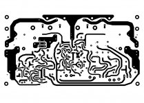
Godfrey - Moving the Zobel is not so easy, as everything else will also have to be moved. Is there any reason why having this current path open is so important? There are many other paths (very thick traces of the ground plane) where the current can travel. Just curious. Even if the Zobel is moved, this track will never be as thick as some of the others, so the current will mostly flow the other way regardless.
Last edited:
Not trying to be combative or dense here, but doesn't this method just place the resistors across the two source bolts of each mosfet? Wouldn't you need to put the resistor from source to output? Wouldn't you would need to cut the trace around the bolt that connects source to output?
If you isolate the bolt that is connected to the output from the case, and then connect the the two bolts (the other bolt is not isolated from case) with a source resistor then I think you have achieved what you are after.
No, just the zobel. See 2'nd pic in post 35.Godfrey - Moving the Zobel is not so easy, as everything else will also have to be moved.
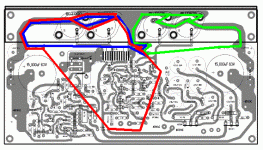
Yes, but only round the front of the board near the input, not across the back. The middle section (colored red in first pic below) is very dense, with no current paths across from left to right. That's why I was trying to open up a path across the top.There are many other paths (very thick traces of the ground plane) where the current can travel.
Yes, at low frequencies. I was thinking of high frequency stability. Second pic below shows the high frequency current paths for the output devices. Green on the right is for the P-channel devices. On the left, red shows (roughly) the old path for the N-channel devices, and blue shows how it is with a copper track across the top.Even if the Zobel is moved, this track will never be as thick as some of the others, so the current will mostly flow the other way regardless.
Reducing the area of those loops is a good idea as they are effectively inductors in series with the decoupling caps. That's also why I suggested moving the decoupling caps - to reduce the loop areas, which reduces the inductance.
I'll admit I'm just being picky with all of this.
It will probably work fine as it is.``````````````````````````
[OT]
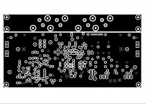
If I was building something like this, I would consider extending the copper ground plane to the top of the PCB, under the bracket. Since the heatsink needs to be earthed anyway, it might be a good idea to do it right there, with the bracket bolted directly to the ground plane.
A safer option would be to have a separate copper section under the bracket, with a thin dividing line between that and the rest of the ground plane. Then you'd have the option to bridge them with solder (or not), depending on preference and the overall grounding scheme.
[/OT]
Attachments
Submitted the PCB layout to a PCB manufacturer for a quote. I'm ahead of schedule! I should be able to place the order by the end of this week, or early next week.
Final board specifications:
- FR-4
- 1oz. cu.
- Lead free solder finish
- Plated holes
- 2 layer (double sided)
- No silkscreen printing
- No solder mask
- No solder paste mask
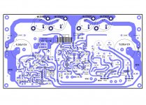
Here are the pictures:
Final board specifications:
- FR-4
- 1oz. cu.
- Lead free solder finish
- Plated holes
- 2 layer (double sided)
- No silkscreen printing
- No solder mask
- No solder paste mask
Here are the pictures:
Attachments
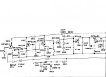
Can the 2SK134 / 2SJ49 MOSFETS be used as the outputs instead? It looked like one of the pictures of the Goldmund 3 had these as the output transistors.
Thanks, Daniel
yes, the original used these.
- No silkscreen printing
- No solder mask
- No solder paste mask
May I ask as to why you are not choosing a solder mask, and (much more importantly, in my mind) no silkscreen stuffing guide???
I have a wonderful Borbley phono stage that is currently on hold because the PCB is not silkscreened, and the stuffing guide is woefully inadequate.
Even if there are errors on the silk, a revision page and note of changes will be able to address any problems.
I humbly, but strongly suggest a silkscreen stuffing guide on the PCB. I am sure I am not the only one who would also like this.
DanFrank - Yes.
6L6 - I like the option to solder anything I want anywhere on the ground plane. Solder mask is a pain to remove and after it's scrapped off, it looks like garbage.
Silkscreen is useless. You have the layout right in front of you. Plus without the solder mask, it would have to be printed directly to the tin plated ground plane, making it look ugly.
Silkscreen is quite nice to have, IMO, especially when you are hand soldering.
I still have your boards in good memory. Beside cviller's jobs, the best boards I've ever seen.

Personally I think it's unpractical to have the values printed since it's hard to make a design with fixed values, much better to only have the designators, R1, R2 etc.I think so, too,
but you can do it in a way, the values / component's names are hidden, once they are soldered:
An externally hosted image should be here but it was not working when we last tested it.
Best regards - Rudi_Ratlos
Goldmund Mimesis 3 Clone's Part List
Here's the entire complete parts list. The only items that are not included are chassis' hardware (aluminum bar stock plates, bolts, nuts, washers, nylon washers, locking washers, etc.). My next post will be pictures of the raw PCBs. I should get them in the next week, or so.
Here's the entire complete parts list. The only items that are not included are chassis' hardware (aluminum bar stock plates, bolts, nuts, washers, nylon washers, locking washers, etc.). My next post will be pictures of the raw PCBs. I should get them in the next week, or so.
Attachments
-
Goldmund Mimesis 3's Part List.txt10.7 KB · Views: 704
-
 Goldmund Mimesis 3 Schematic .jpg489.1 KB · Views: 2,621
 -
 Goldmund Mimesis 3 Protection Schematic 1.jpg186.3 KB · Views: 2,397
 -
 Goldmund Mimesis 3 Protection Circuit 2 .jpg125.5 KB · Views: 2,192
 -
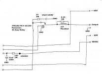
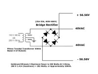 Goldmund Mimesis 3 Power Supply Schematic .jpg260.8 KB · Views: 1,185
Last edited:
- Status
- Not open for further replies.
- Home
- Amplifiers
- Solid State
- Goldmund Mimesis 3 Clone, World's Best Amplifier!!!!