Hi guys, i am thinking of building 2+ CM for the First One modules. I will be using 45VAC so VDC would be about 63V or so after rectification and with voltage output aim about 60V with 0.7V reduction. I have bs170 and bs250 but yet to work out other changes required for the suitable voltage output. Any suggestions guys?.
Quan
Quan
Need Help
Hello guys,
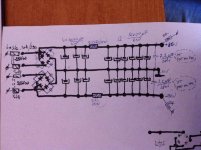
This year i managed to make some money to buy myself two trafos E+I 300VA@25+25v@5A bifilar secondaries windings for the a dual monos Jean Hiraga 30w "Super Class A amplifier". I want to make a separate 25-0-25V for the input and 30-0-30V just for the output tranies.
Wich solution is better for the best sound quality:
1. The schematic attached (one per single chanel) but with Mr Evil CM instead of the 0.22Ohm/25W resistors for the outputand another CM for the input.
2.The schematic attached as it is (one per single chanel) for the output and a separate Mr Evil CM for the input.
* Can i use a single CM for both inputs from a separate trafo (20+20VA)? Or i have to use separate CM for each channel?
*What is better to use: a separate trafo for CM of the input or take the AC current from the same trafo used for the input?
Thanks in advance
Hello guys,
This year i managed to make some money to buy myself two trafos E+I 300VA@25+25v@5A bifilar secondaries windings for the a dual monos Jean Hiraga 30w "Super Class A amplifier". I want to make a separate 25-0-25V for the input and 30-0-30V just for the output tranies.
Wich solution is better for the best sound quality:
1. The schematic attached (one per single chanel) but with Mr Evil CM instead of the 0.22Ohm/25W resistors for the outputand another CM for the input.
2.The schematic attached as it is (one per single chanel) for the output and a separate Mr Evil CM for the input.
* Can i use a single CM for both inputs from a separate trafo (20+20VA)? Or i have to use separate CM for each channel?
*What is better to use: a separate trafo for CM of the input or take the AC current from the same trafo used for the input?
Thanks in advance
Attachments
Are there any further revisions to the design to incorporate the suggestions/improvements from the last few pages, or are they impossible to incorporate because the PCB would then turn into something that cannot be etched?The main ground bus was a copper "pour", I removed it temporarily. With this software, it is easier to put those in last, because once the copper is laid it takes extra effort to move components around.
If I am following your earlier comments correctly, then there are actually two different ground nodes left to connect. (C3, R3, R11) is one, and R9 is the other one, the one associated with the feedback node.
I am not sure what you mean by "measuring ground", but I assume that is R9, or what I have been calling feedback.
R9 can be rotated 90-degrees to put one end closer to the output ground terminals (C9 can be moved to make room for that, I just did not do it in the last post). If that is done, then there will be room for a separate trace to the output GND terminals.
The board is actually 2-sided w. plated holes now, but I want people to be able to etch it themselves if they want to. That was the point of the layout you first commented on. I have no objection to a few top layer traces.
post584 shows an rCRC PSU.
That gives a low ripple supply with an output voltage that tracks (follows) the mains voltage.
If you want two sets of voltages to supply different parts of the circuit:
Do as the tube/valve builders do it.
rCRCRCRC and tap off different voltages at the different C tappings of the PSU.
The highest voltages are at the beginning and the lowest voltage is at the end of the string.
BUT
the end of the string has current supplied through many Rs, whereas the beginning of the string has current current through only the little r of the transformer.
Draw a big current from the little r and draw a low current from the many R+R+R.
If you need the big current AND low voltage from the end of the string then all the R+R+R run hot and the output voltage varies a lot, not following/tracking the mains voltages. The output voltages varies with the current drawn by the amplifier. Equals bad PSU.
If you draw the Big current at the beginning and draw a near constant low current from the end you have a good PSU.
If you need low current at high voltage and high current at low voltage then BUILD TWO PSUs.
Last edited:
Thank you very much Andrew. I'll build myself another PSU for the input with this CM.
Is it ok to feed both inputs from a single CM and the outputs from separate psu-us? Will they oscillate like hell in this scenario or work like charm?
I want to know if i have to build two, each for both channels or one for both of the channels..
Thanks in advance
Is it ok to feed both inputs from a single CM and the outputs from separate psu-us? Will they oscillate like hell in this scenario or work like charm?
I want to know if i have to build two, each for both channels or one for both of the channels..
Thanks in advance
Last edited:
I want to layout the CM with 100mm x 100 mm and use parts that I have on my pocket. So I did a single side layout of CM. But I'm not sure about the quality of my layout.
I will attach it here so may be some one can correct / point out what missing.
Thanks!
I will attach it here so may be some one can correct / point out what missing.
Thanks!
Attachments
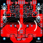
1) There might be just enough room to route the tracks between the fuses and pass transistors on the inside of the heatsinks, reducing the loop area between them and ground. To do that, you would have to swap the fuses with the LEDs, so the fuses are next to the capacitors and the LEDs are at the edge of the board, and flip the IRF9540 so it's on the left side of the heatsink.I want to layout the CM with 100mm x 100 mm and use parts that I have on my pocket. So I did a single side layout of CM. But I'm not sure about the quality of my layout.
I will attach it here so may be some one can correct / point out what missing.
Thanks!
2) You might struggle to get to that connector between the reservoir capacitors. The other two between capacitors and diodes might be fiddly too.
3) The diodes are very close to the capacitors. It's not a big deal because they don't give off much heat, but it's better to keep electrolytic capacitors as cool as possible.
4) Make sure the screws you use in the mounting holes don't touch the heatsinks.
Hi,
The connector between caps are for a single wire connect to star ground outside the board.
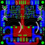
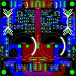
I updated my layout as you recommend. I switched to two sides layout. Could you have a look at it?
The connector between caps are for a single wire connect to star ground outside the board.
I updated my layout as you recommend. I switched to two sides layout. Could you have a look at it?
Attachments
Last edited:
Seen many times documented better noise figures when sence points taken as near as possible to load, as is will also work but consider the suggestion. Marked at attached picture 9 white star places that should have own trace or shared trace enroute to yellow star and that you switched to two layer layout should help this. Between the four output GND spades at top of PCB down to 10mF capasitors there's dirty heavy current flow that sence points now avoid sitting in middle of now being more downstream to load and sence at the same point. See some of same in picture of PCB by Mr Evil at post #1.Hi,
The connector between caps are for a single wire connect to star ground outside the board.
I updated my layout as you recommend. I switched to two sides layout. Could you have a look at it?
Attachments
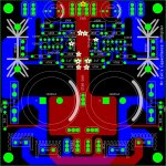
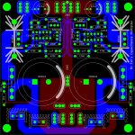
Here is an update of my layout. I connect all ground point to a single point then connect to the yellow star point.
Very nice layout!
Are you planning a GB? What will be the max voltage and current supported in your version?
Thanks
Do
Very nice layout!
Are you planning a GB? What will be the max voltage and current supported in your version?
Thanks
Do
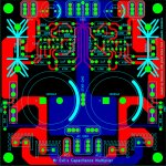
I don't have any plan for a GB. It is for my selection parts. But if someone want to start one, I can provide him my files. With my current devices, the max voltage will be +-40V, it is because of the small signal mosfet can't take more voltage.If you use higher limit mosfet, it can be increase.
Attachments
Hi obscurus nice work!I don't have any plan for a GB. It is for my selection parts. But if someone want to start one, I can provide him my files. With my current devices, the max voltage will be +-40V, it is because of the small signal mosfet can't take more voltage.If you use higher limit mosfet, it can be increase.
If it is for sharing, post pdf here
")
I don't have any plan for a GB. It is for my selection parts. But if someone want to start one, I can provide him my files. With my current devices, the max voltage will be +-40V, it is because of the small signal mosfet can't take more voltage.If you use higher limit mosfet, it can be increase.
Are you planning to have the board(s) commercially fabricated? If so, most of the costs will be fixed set up costs) regardless of the number of boards you order, in other words, the more boards you order the lower the cost of each board. If you were to order more boards and offer them for sale your own boards would be a lot cheaper and you would help others; I would probably order a couple from you. Just a thought.
Ray
Could you include a 'ground loop isolating resistor', or thermistor, next to the 4 way connection point at the top of the board, so the 'ground' wire to the earth point on the chassis can just be a direct connection - much simpler ....
I think the 'ground loop isolating resistor' must be connect to the center ground point (between two big caps) rather than at the top of the board?
@nautibuoy: Sorry, I don't want to start a GB on it. May be someone else ... My PCB will be process by a PCB company which have nice price for qty of 5.
@thimios: I will post PDFs file when it is finalize. I'm also going to make board, test and will let everyone know results.
@pinnocchio: I think I'm wrong about max voltage with current part choose.
The maximum voltage depend on
- Big cap voltage rate ~ Vp
- Output cap. ~ Vp
- Mosfet max voltage ~ Vp / 2
- Jfet max voltage ~ Vp / 2
Last edited:
Here the latest layout with pdf files attached (not mirrored). There are only some smalls change.
Attachments
- Status
- This old topic is closed. If you want to reopen this topic, contact a moderator using the "Report Post" button.
- Home
- Amplifiers
- Power Supplies
- Finished capacitance multiplier