Well done - that shows good lateral thinking in your layout - Great stuff - we can all learn something from this as most of us get set on particular ways of doing routine things like similar diode bridges, etc
Perhaps if you're in mind of a bit of a 'play around', maybe shift those leds next to your existing '0V' tab - these leds are really an indicator of the voltage across the big capacitors, so can connect them in parallel to these caps, no separate track to the 'STAR GND" at all - bit simpler.
This allows you to move the fuses and the big caps out a couple of mils and then move the AC GND tabs back towards the space between the big caps, maybe one in front of the other instead of side-side - need to solder the tabs in before the big caps.
This allows you to bring the AC tabs back towards the centre and front edge of the pcb with enough offset between them for easy pushfit and have enough room to fit the Rs + Cs caps between the AC tracks and the ground plane - the Cx caps can easily be added underneath if too crowded.
Those diodes can be nearly lined up again for a simple flat bar heatsink.
I have a question about using the IRF540/9540s - If I remember right, these fets have a Vds of about 4.5 volts, yes? So, a current thru the filter of about 1Amp will generate about 4.5W of heat and will the sinks be big enough to keep them cool enough?
I'm a bit of a 'throwback' with this ground plane stuff but one thing I do REALLY DISLIKE is the way the pcb programs just don't allow enough clearance space between the top mounted components and the top layer - whenever I get stuck with this situation, I end up making my own clearance space and it generally looks untidy, but works!
Looking good,
and as '454' said, add your name on it - it's your thinking.
If 1A current get through fet, and voltage drop is 4.5V then it will be 4.5W of heat but
- 1A is peak current (max), I think with normal music play, it is much lower value (current).
- 4.5V is Vgs not Vds, I think voltage drop = Rds on * I? And we have the VR to change it? When sim using LTSpice, I can adjust VR to get 2V drop with 40mV ripple on 3A current (fet Rds on = 40 mOhms).
- 1A is peak current (max), I think with normal music play, it is much lower value (current).
- 4.5V is Vgs not Vds, I think voltage drop = Rds on * I? And we have the VR to change it? When sim using LTSpice, I can adjust VR to get 2V drop with 40mV ripple on 3A current (fet Rds on = 40 mOhms).
Last edited:
Well, I have never been totally comfortable about adding a ground plane around noisy diodes and tying it back into the power supply main GND point (STAR GND, Audio GND, etc) but other people (and much smarter) say it's a requirement to reduce radiated noise, so I tried one design with the unconnected top layer area around the diodes, caps, etc and directly connected it to the chassis earth, but it didn't seem to make any difference to the sound so ... (but that just my 'take' on it - it's easy enough to add it)
Remember that the AC GND tabs only connect the centre of the windings to the caps centre point and some point of reference GND - 4 points and the snubber caps, 2 x Cs & Cx.
If you drop out the top layer from the central 0V tab (for the moment) and connect the diodes directly to the caps pins and add those 'pesky' AC GND tabs close to the junction between the caps, maybe one 'above' the other (= a simple triangle), and then move the thick AC1 and AC2 bottom layer strips towards the bottom edge of the board, there's now plenty of room to arrange both the snubber parts and bring the diodes closer together thus shortening the whole tracks, etc and then you can add the ground plane where you choose (if so, please see if you can leave a bigger clearance between the non conducting tabs, etc - not sure if program allows any choice)
Moving the indicator Leds to the centre also gains you a bit more freedom and these are attached to the power cap ground point, not the Star ground, as it's 'dirty power'.
You might offset the diode heatsinks if retaining separate heatsinks as a bit awkward to assemble this close together - they don't have to be symmetrical about any centre point just to look neat either
Oh, a small thing - the case of some electrolytic caps is connected to the cap's negative pin so, case with the new position for the AC GND tabs near the power caps (if you go that way!), allow a couple extra mm for clearance from the right hand power cap in case the plastic insulation gets scratched/torn and shorts to neg rail - same with heatsinks
I'd rather play with this 'stuff' than do the Sudoki puzzles!
It's good practice for lateral thinking, or any thinking for that matter, as many engineers are noted for narrow focus & ridgidity in problem solving (notorious, actually!) as they 'gain experience' as they say.
All the best ...
You got some point. I think we cant have everything good, that's not possible. Base on what you recommend, I did a new layout.
I think with this layout, I can make the move ground line to bottom panel. And make other ground trace top panel?
--> Is it the 220uf and the 10000uf cap.
I think with this layout, I can make the move ground line to bottom panel. And make other ground trace top panel?
Oh, a small thing - the case of some electrolytic caps is connected to the cap's negative pin so, case with the new position for the AC GND tabs near the power caps (if you go that way!), allow a couple extra mm for clearance from the right hand power cap in case the plastic insulation gets scratched/torn and shorts to neg rail - same with heatsinks
--> Is it the 220uf and the 10000uf cap.
Attachments
I think I first recall Cherry indicating the subtlety of taking AC GND terminal through two independent traces to each 1000uF cap pad, and then use another two independent traces from the cap pads to your 0V point. That separates the rectifier currents from the amp signal currents as much as practical - without trying to source 4-terminal caps ") .
.
.That looks a lot simpler and you can still spread out that AC GND top layer into a ground plane if you want.
You'll laugh at this weird idea - on the previous CMx pcbs, I cut the main track between what you call the '0 V tab' and the 'Star GND' and added a 0.1 Ohm 3 watt SMD resistor and the whole supply is a bit quieter, would you believe! I get quite a few comments about that, but it does makes sense! (I tried adding a simple CMx in the gnd track but this didn't work out too well with the usual '4 diode bridge per transformer winding' system I use..)
I see you moved the Led connection okay - I forgot about the last pcb design used a fuseholder that has the 3mm Leds poking up thru the middle, under the fuse - looks rather neat, too!
I would suggest you shorten the long traces hitching the Cx and Cs (a bit of a disaster, that!)- not too hard actually -
Push the AC1 and AC2 tabs apart until they're about the position of the Cx caps, then pull the centre 2 diodes to the lower, now vacant space and position the 2 pairs of Cs & Cx above them and attach them to the AC GND point - the resistors Rx can simply attach to the big +/- tracks going from the diodes to the ripple caps (the 10,000uF ones) - you can position it nearly all the way across the outside of the track to fit it in or alter that big track a bit -
Ah, just saw this - when you move the Cs + Rs at the end of the heatsink strip, you can leave a bit more room between those 2 central diodes and fit all 4 caps in the gap - they're not very big size (MKS filter caps, not the bigger Propylenes and only 63 volt ones)
Your whole top part of the board now has some more room to spread the components about if you want to - not really necessary.
If you want to mount the IRF540 fet from the outside, just change the gate and pins around - how's that gate track attached? Might add a double donut or something for possible later repair - looks a bit incomplete, or something
Looking good - a bit surprising that you're not getting some other comments - there's a lot of ways of designing pcbs and there's a lot of smart people here that probably have different, and quite probably better, ideas
Remember that my ideas about pcb design makes perfectly good sense to me, but is no guarantee it's anywhere near 'the best' way - 'old heads' are no guarantee of 'smarter thinking', just look at our politicians! (couldn't resist that one!)
I think I'm talking rubbish (again!) about this Neg terminal attached to the outside metal can - I just tried some Nichicons, Silmics Panasonics, Mundorf, etc (anything pcb mounting) and none have the neg terminal connected - so, please ignore my comments - some of the older screw terminal heavy duty caps like BHC, Siemens, Rifa etc have this to help the cooling of the cap's case and internals.
Jeez, someone else that remembers 'big Ed' - yes, he had a 'thing' about this separation of currents, ground plane returns, etc - another 'rather bright' guy.
I'm not sure why "two" traces in and "two" traces out.I think I first recall Cherry indicating the subtlety of taking AC GND terminal through two independent traces to each 1000uF cap pad, and then use another two independent traces from the cap pads to your 0V point. That separates the rectifier currents from the amp signal currents as much as practical - without trying to source 4-terminal caps
Not just Dr Cherry.
Most that understand the need to separate the charging circuit from the audio circuit ensure that "one" trace never shares different types of current flow/return.
lots of ways indeed. There is another Thread running discussing the same topic. And it's in many older Threads.................. - a bit surprising that you're not getting some other comments - there's a lot of ways .........
@jameshillj: Your recommend sound reason-able to me that's why I'm a bit more addict to your words.
I wouldn't try the SMD trick, not here and now but I can experiment later. Is this some kind of ground breaker resistor method?
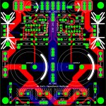
Again, I updated the layout. I feel no problem with IRF540 not face outside so I leave it there. I tried to make some extra space and fit Cs, Cx, Rs near the AC GND area. They are overlap but I think I can solder Cs, Cx at the bottom. I will later apply a ground panel to GND when others thing are so-so. I add two connect for AC Ground because there are transformer with two secondaries, have one terminal will make it harder in this case.
I also not sure about the 220uf cap at output. Do you think connect it to output terminals sound fine?
A picture worth thousand words. Here is the layout.
I wouldn't try the SMD trick, not here and now but I can experiment later. Is this some kind of ground breaker resistor method?
Again, I updated the layout. I feel no problem with IRF540 not face outside so I leave it there. I tried to make some extra space and fit Cs, Cx, Rs near the AC GND area. They are overlap but I think I can solder Cs, Cx at the bottom. I will later apply a ground panel to GND when others thing are so-so. I add two connect for AC Ground because there are transformer with two secondaries, have one terminal will make it harder in this case.
I also not sure about the 220uf cap at output. Do you think connect it to output terminals sound fine?
A picture worth thousand words. Here is the layout.
Attachments
I'm not sure why "two" traces in and "two" traces out.
AC GND terminal has one trace to one of the 1000uF cap pads, and another trace to the other 1000uF cap pad. Then a trace runs from each cap pad to the 0V point. There is no direct trace connection from AC GND to the 0V.
Yes, the resistor in the return path acts like an isolator and a peak current reducer - I normally use a similar resistor between the diodes and the ripple caps as it makes a smoother sound without losing any 'punch' or transients, etc - very common, but another distraction - an easy one to play with later if you want.
I wouldn't worry about the output caps and any possible touching of the cases - if you want to try bigger/different ones, just add them below - my CMxs for the F5 amp have a couple of those large Nichicon SuperThru caps on the output and I 'mounted them' underneath the pcb and with long standoffs for clearance - works like a charm.
As Mr Robbins mentioned, it's quite easy to apply the separate trace idea - it makes a diamond shape between the AC GND tabs, the 2 capacitor pins and the 0V tab - QED - I'd forgotten about this - I learn, or re-learn, something everyday, eh!
Pinnocchio also has a valid point about using a complete bridge (4 diodes) for each winding and is something to be recommended, or a block bridge for simplicity.
However (isn't there always a 'but' somewhere!), soft recovery block bridges like the excellent IXYS ones aren't all that cheap, but simple to assemble/fix - the 'but' comes in when you need to mount the snubbers on the bridge's terminals for the required direct connection to the secondary transformer windings use - hmm, a conundrum, eh!
I generally use separate diodes (8 of them on a heatsink - silly idea about extra shielding!) and tightly twist the wires to the caps - this is where I add those series resistors and the snubber components - in engineering terms, it's not ideal by any means, but it seems to work in practice - that's my 'excuse' anyway (I get lazy too!)
So, how can we include the options to include all this in the limited size pcb?
I don't think you can, or even if you wanted to - I think your layout/version of Miles' design will work perfectly well, just as it is ...
About that layout -
With a bit of shuffling around of the diodes (add a bit more space in the centre, and move the outside onesinto the space near the fuses, maybe) can create enough extra space to line up those snubber caps and resistors in a row and at the same time, pull the 2 AC GND tabs away from the fat capacitors, to enable easy assembly, etc and still make a 'diamond' shape of the ground tracks -
It's fun, eh - a bit like painting, I think - I can see how some people get very frustrated by the exercise.
Actually, looking at it again, it might be possible to tuck 2 block bridges onto the end of the board if you shift the mounting holes towards the fuses - maybe on their sides with short wires to the pcb if necessary, and the heatsink(s) vertical off the end of the pcb ....
But, not, NOT, the cheap GB bridges - they're pretty ghastly (bloody awful!) for sound quality - and you can't get rid of the 'hash', even thru the CMx, filters, anything.
Oh, the idea about changing the Fet around was that using a threaded hole in the heatsink, it makes it easy to replace them from the outside if you kill them (or probably 'when', for me!)
If you wanted to allow for more options with part footprint, then I guess the 1000uF cap would be a reasonable target given the plethora of available cap size formats from different manufacturers. Perhaps allow for two caps in parallel of smaller diameter as well as the original single large diameter cap - that looks a pretty simple mod where the two caps are located north and south of existing pads.
And are you using both sides of the board for the main current traces where there is no conflict, or just using the red side?
And are you using both sides of the board for the main current traces where there is no conflict, or just using the red side?
Last edited:
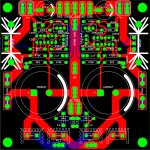
I think I could split the layout to two: one for 4 diodes and one for 8 diodes so I can select which one suit better on specific case. I have transformers that have two secondaries and transformers that have one secondary with center tap.
About the diode bridge, I'm not familiar with them, could you recommend one? I have some local company have Taiwan BR3510, is it ok since it is quite cheap 1$ / 1 pc.
And here the layout, again (x times) I will go with four diodes first. Is the AC GROUND tabs look fine? I swear it does not look like any diamond to me And with this config, transformer with one secondary with center will have some drawback? since it have only one ac ground tab.
About the diode bridge, I'm not familiar with them, could you recommend one? I have some local company have Taiwan BR3510, is it ok since it is quite cheap 1$ / 1 pc.
And here the layout, again (x times)
I will go with four diodes first. Is the AC GROUND tabs look fine? I swear it does not look like any diamond to me And with this config, transformer with one secondary with center will have some drawback? since it have only one ac ground tab.Attachments
Last edited:
But, not, NOT, the cheap GB bridges - they're pretty ghastly (bloody awful!) for sound quality - and you can't get rid of the 'hash', even thru the CMx, filters, anything.
Hi JH,
Which quality square bridge are you referring to? I have a new project and it could be useful to find a good quality one.
Thanks
Do
Okay, the diode bridge first - the only ones that I got serious about were the IXYS ones - 20A, 600V with a relatively slow Trr of about 80nS but sounded very similar to the soft recovery diodes I normally use - they have a Vf of about 2 volts (a voltage drop of about 2 volts across the diode) so need a good heatsink - diodes like this like to stay as cool as possible
The $18 price tag is a bit of a shocker but each soft recovery diode usually comes to about $3+ so not so bad - flat pack, 5 pins - easy to setup - looked up the number = FBE 20-06N1 - no doubt other similar ones around but the 'lazy me' just got into gear!
Back to 'the puzzle' - Hmm, I wouldn't have done it that way - put the 2 AC GND tabs together in between the 2 Rs resistors in the the middle of the 'snubber pack' and just the 1 track from there to each cap pin, to form the bottom half of the diamond shape - and from each of these same cap pins, run a track up to what's labelled as the 0V tab (and ignore that tab between the 2 caps) to form the diamond that Ed Cherry advocated - some people do disagree with the idea and not sure if it makes all that much difference in practice
If you want to play around with the flat pack IXYS diode block, there isn't any reason, apart from convention, that you need to keep any of the 5 pins in the one line - I bent them all around the place to keep the tracks much simpler and it was surprisingly quite neat! I routinely do the same thing with transistor and Fet legs and can't see any reason 'why not', but a lot of people just hate it as it's unconventional and just not tidy, or something!
Oh something else you might want to look at - the AC input tabs could be a bit further away from the heatsinks as a couple of those heatsinks sit directly above the top layer tracks - not a big deal, but ...
Are the '+' and '-' tabs on the top of the board (output tabs) 5mm apart, so can possibly fit screw terminal blocks - same with all those central ground tabs?
Interestingly, now that most of the tracking has gone to the bottom layer, you can spread that ground plane all over the top area without hindrance, if you want - serendipity, or something!
- Status
- This old topic is closed. If you want to reopen this topic, contact a moderator using the "Report Post" button.
- Home
- Amplifiers
- Power Supplies
- Finished capacitance multiplier