Okay, the diode bridge first - the only ones that I got serious about were the IXYS ones - 20A, 600V with a relatively slow Trr of about 80nS but sounded very similar to the soft recovery diodes I normally use - they have a Vf of about 2 volts (a voltage drop of about 2 volts across the diode) so need a good heatsink - diodes like this like to stay as cool as possible
The $18 price tag is a bit of a shocker but each soft recovery diode usually comes to about $3+ so not so bad - flat pack, 5 pins - easy to setup - looked up the number = FBE 20-06N1 - no doubt other similar ones around but the 'lazy me' just got into gear!
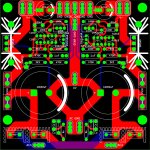
Back to 'the puzzle' - Hmm, I wouldn't have done it that way - put the 2 AC GND tabs together in between the 2 Rs resistors in the the middle of the 'snubber pack' and just the 1 track from there to each cap pin, to form the bottom half of the diamond shape - and from each of these same cap pins, run a track up to what's labelled as the 0V tab (and ignore that tab between the 2 caps) to form the diamond that Ed Cherry advocated - some people do disagree with the idea and not sure if it makes all that much difference in practice
If you want to play around with the flat pack IXYS diode block, there isn't any reason, apart from convention, that you need to keep any of the 5 pins in the one line - I bent them all around the place to keep the tracks much simpler and it was surprisingly quite neat! I routinely do the same thing with transistor and Fet legs and can't see any reason 'why not', but a lot of people just hate it as it's unconventional and just not tidy, or something!
Oh something else you might want to look at - the AC input tabs could be a bit further away from the heatsinks as a couple of those heatsinks sit directly above the top layer tracks - not a big deal, but ...
Are the '+' and '-' tabs on the top of the board (output tabs) 5mm apart, so can possibly fit screw terminal blocks - same with all those central ground tabs?
Interestingly, now that most of the tracking has gone to the bottom layer, you can spread that ground plane all over the top area without hindrance, if you want - serendipity, or something!
Actually, there's an exact version of what you just put on top but 22A for half the price. Look for FBE22-06N1
That would be great to have two like those per PCB. Pins are almost 4mm center to center so it is quite easy to align all pins.
Do
Now I know why your guys mean diamond shape ") It does look like one. So I applied it.
It does look like one. So I applied it.
I added some more space for AC1 & AC2. I also checked my connector, it should fit without touching the heatsink. The heatsink in my design are very light and will float in the air so it will never touch the pcb top layer.
It does look like one. So I applied it. I added some more space for AC1 & AC2. I also checked my connector, it should fit without touching the heatsink. The heatsink in my design are very light and will float in the air so it will never touch the pcb top layer.
--> will do after everything are ok.Interestingly, now that most of the tracking has gone to the bottom layer, you can spread that ground plane all over the top area without hindrance, if you want - serendipity, or something!
--> They are 5.08mm by luck. I was not intended to make them that way.Are the '+' and '-' tabs on the top of the board (output tabs) 5mm apart, so can possibly fit screw terminal blocks - same with all those central ground tabs?
--> I don't understand how to do that. Could you explain more detail about it?Oh, the idea about changing the Fet around was that using a threaded hole in the heatsink, it makes it easy to replace them from the outside if you kill them (or probably 'when', for me!)
Attachments
You might need to change the track from the Right hand side fuseholder to the IRF540 Fet as the pads for trhe Fet when you turn it around are closer to the outside of the pcb and the fuseholder <-> Fet track goes to the 'top' pin now, not the 'bottom' pin - the gate is straight into the 8R2 resistor now, and can go back to 'bottom layer track', too.
Also, strange tho it may seem, you could quite easily move all the components at the top of the board away from the centre ground track and run that big one from the 0V tab to the STAR GND tab (reduced to about half) right down the middle - this allows the top layer ground tracks to go back to the bottom layer also - same with any other unnecessary top layer tracking
Why, you ask?
Well, in years to come, people are going to be making these pcbs and if it's already nearly a single layer pcb, guys can knock them up at home to their hearts content and the humble CMx will become a staple addition to basic power supply building blocks, complete with transformer snubbers, etc, etc, and will have YOUR NAME ADDED as the pcb designer too, along with Miles' as the cct architect. (on top mask/bottom layer reversed)
Are you feeling rather swamped with other directions/pressure by now?
What I do is take a break and come back to it in a day or two and have a fresh look and then see about changing things again if you are uncomfortable with anything at all (and tell us all to 'bugger off' with all the yadda, yadda!)
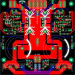
Incidently, what is the outside measurements of the whole board - it looks to be about 100 x 200mm (4" x 8")?
I had a brief look at Dominic's suggestion of using 2 of those FBE 22-06N1 IXVS bridges and it's quite a simple work-around if the left hand bridge has it's pin 1 facing left and the right hand bridge has it's pin 1 facing right, then the 2 AC1 and AC2 are right in the bottom centre and the '+' and '-' tabs are on the outsides and easy to feed them directly to the cap pins -a simple bar heatsink can be placed right across the board with the 2 bridges attached to either side of the bar/heatsink (or the pins get bent a bit) and no insulating washers needed - pretty neat, huh! He's a smart guy.
At the cost of 2 x $7, this isn't much more expensive than 4 diodes, sinks, nuts, bolts, etc, (and all bottom layer too, I think!)
Domestic chores beckon - grass mowing - have to earn that cold beer!
Also, strange tho it may seem, you could quite easily move all the components at the top of the board away from the centre ground track and run that big one from the 0V tab to the STAR GND tab (reduced to about half) right down the middle - this allows the top layer ground tracks to go back to the bottom layer also - same with any other unnecessary top layer tracking
Why, you ask?
Well, in years to come, people are going to be making these pcbs and if it's already nearly a single layer pcb, guys can knock them up at home to their hearts content and the humble CMx will become a staple addition to basic power supply building blocks, complete with transformer snubbers, etc, etc, and will have YOUR NAME ADDED as the pcb designer too, along with Miles' as the cct architect. (on top mask/bottom layer reversed)
Are you feeling rather swamped with other directions/pressure by now?
What I do is take a break and come back to it in a day or two and have a fresh look and then see about changing things again if you are uncomfortable with anything at all (and tell us all to 'bugger off' with all the yadda, yadda!)
Incidently, what is the outside measurements of the whole board - it looks to be about 100 x 200mm (4" x 8")?
I had a brief look at Dominic's suggestion of using 2 of those FBE 22-06N1 IXVS bridges and it's quite a simple work-around if the left hand bridge has it's pin 1 facing left and the right hand bridge has it's pin 1 facing right, then the 2 AC1 and AC2 are right in the bottom centre and the '+' and '-' tabs are on the outsides and easy to feed them directly to the cap pins -a simple bar heatsink can be placed right across the board with the 2 bridges attached to either side of the bar/heatsink (or the pins get bent a bit) and no insulating washers needed - pretty neat, huh! He's a smart guy.
At the cost of 2 x $7, this isn't much more expensive than 4 diodes, sinks, nuts, bolts, etc, (and all bottom layer too, I think!)
Domestic chores beckon - grass mowing - have to earn that cold beer!
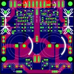
From my faulty understanding about ground planes, I think you need to separate the plane around the diodes/capacitors, etc from the rest of the active circuit and send this section of the ground plane directly to chassis earth point, and not the STAR GND at all - this leaves the ground plane surrounding the other active components to be connected to the main STAR GND - there's a division, or gap, in the ground plane near the ripple capacitors - IIRC, there's some clear explanations about this on the Tent Labs site.
.... my rather vague thoughts, sorry.
The rest of the layout looks pretty complete - jeez, 100 x 100mm, it's a pretty compact little fella!
.... my rather vague thoughts, sorry.
The rest of the layout looks pretty complete - jeez, 100 x 100mm, it's a pretty compact little fella!
I'm interested in this as a potential supply for a Linsley-Hood class A amp I'm planning to put together; can you remind me of the voltage current range this is specified for? I would need to deliver 24V @ around 1.7A.
Some observations on the layout below.
Thanks for progressing this.
Ray
I would suggest something quite the opposite; rotate the left hand IRF9540 and it's associated heatsink through 180degrees so that the device's mounting tab faces outwards. That way will give more flexibility as you could then have the option of mounting the devices from under the board onto a chassis heatsink. If you want to make them easy to replace when oriented that way 'on board' just use the mounting nuts and bolts 'the other way around' or use allen bolts. Rotating the left hand device will involve moving some tracks but it shouldn't be difficult.
If you swap over the diodes first and second from the left then, with a little adjustment of the snubber components, all of the AC tracks can be on the bottom layer of the board (and it will look nice and symmetrical).
Some observations on the layout below.
Thanks for progressing this.
Ray
Oh, the idea about changing the Fet around was that using a threaded hole in the heatsink, it makes it easy to replace them from the outside if you kill them (or probably 'when', for me!)
I would suggest something quite the opposite; rotate the left hand IRF9540 and it's associated heatsink through 180degrees so that the device's mounting tab faces outwards. That way will give more flexibility as you could then have the option of mounting the devices from under the board onto a chassis heatsink. If you want to make them easy to replace when oriented that way 'on board' just use the mounting nuts and bolts 'the other way around' or use allen bolts. Rotating the left hand device will involve moving some tracks but it shouldn't be difficult.
Oh something else you might want to look at - the AC input tabs could be a bit further away from the heatsinks as a couple of those heatsinks sit directly above the top layer tracks - not a big deal, but ...
If you swap over the diodes first and second from the left then, with a little adjustment of the snubber components, all of the AC tracks can be on the bottom layer of the board (and it will look nice and symmetrical).
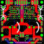
I think this PSU is good for +-14 (since Mr. Evil design it with this voltage - but the jfet must be good under low voltage area = 1/2 * V ) to about +-50V (since it is my limit of cap limit voltage (63V)), and you can choose your components to go to higher limit.
I think +-24V with 1.7A is no problem but class A may need to have bigger heatsink. Since the constant current is high. Let say the voltage drop with fet is 2V so heat will be 2*1.7 = 3.4W.
I'm not change fet location any more. Because my board size is limit. If the track go other way, track size width will be smaller.
--> It's hard to set the AC1 location if I go with this ideal.
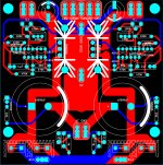
Update layout:
- I decided to not go with ground panel, seem more things to do/research than current star ground.
- I moved the track of ouput cap GND to star ground.
- Added CM name and my name to the board.
I think +-24V with 1.7A is no problem but class A may need to have bigger heatsink. Since the constant current is high. Let say the voltage drop with fet is 2V so heat will be 2*1.7 = 3.4W.
I'm not change fet location any more. Because my board size is limit. If the track go other way, track size width will be smaller.
If you swap over the diodes first and second from the left then, with a little adjustment of the snubber components, all of the AC tracks can be on the bottom layer of the board (and it will look nice and symmetrical).
--> It's hard to set the AC1 location if I go with this ideal.
Update layout:
- I decided to not go with ground panel, seem more things to do/research than current star ground.
- I moved the track of ouput cap GND to star ground.
- Added CM name and my name to the board.
Attachments
Last edited:
Thanks for the info on the boards specification with respect to my possible use.
I think this could be achieved within the board outline and without compromising the track width as you would be able to push the left hand heatsink inwards a little, which would free up some space.
I know you're not planning a group buy for the boards so would it be possible to have the PCB design files so I could make the changes myself t suit my own situation? If so, I might be persuaded to run a one-off group buy to offset the cost of having some high quality boards fabricated, assuming Mr. Evil gives his blessing of course.
Ray
I'm not change fet location any more. Because my board size is limit. If the track go other way, track size width will be smaller.
I think this could be achieved within the board outline and without compromising the track width as you would be able to push the left hand heatsink inwards a little, which would free up some space.
I think it would be really easy, just bring them both to the centre of the board, one in front of the other.--> It's hard to set the AC1 location if I go with this ideal.
I know you're not planning a group buy for the boards so would it be possible to have the PCB design files so I could make the changes myself t suit my own situation? If so, I might be persuaded to run a one-off group buy to offset the cost of having some high quality boards fabricated, assuming Mr. Evil gives his blessing of course.
Ray
Move heatsink back will make them near main caps. It is better to make some separation between them. I think the current placement was not so bad. And it also reduce the loop area between them and ground like Mr Evil said.
AC1 and AC2 doesn't have enough space to place on center. I tried.
About the design files, I can give it to you, no problem on that. Asked me again when I finish it first. BTW, I use Kicad.
AC1 and AC2 doesn't have enough space to place on center. I tried.
About the design files, I can give it to you, no problem on that. Asked me again when I finish it first. BTW, I use Kicad.
Thanks obscurus
I didn't describe this very well and didn't actually mean physically moving the heatsinks; what I should have said is that by moving the device to the other side of the heatsink space is freed up to relocate the tracks.
But no worries, I can make any adjustments I require.
Ray
Move heatsink back will make them near main caps. It is better to make some separation between them. I think the current placement was not so bad. And it also reduce the loop area between them and ground like Mr Evil said.
I didn't describe this very well and didn't actually mean physically moving the heatsinks; what I should have said is that by moving the device to the other side of the heatsink space is freed up to relocate the tracks.
But no worries, I can make any adjustments I require.
Ray
Pcb's availability
Hi there. I've tried building a cap-mult for some time now, using the circuit for the JLH, mirrored on ESP. The revised circuit allow for both output transistors being of the same type. I've made it on proto-board, and in a final attempt, also tried making it by soldering the components together directly. (new and fresh components this attempt ofc).
On both these attempts, I get the same result. I can't adjust the voltage, especially on the - rail. The positive one stays at 18V with a 320 ohm 5W resistor, the - one drops to 9 volts.
So I'm kinda ready to give up.
Does anyone have pcb's for this circuit or a better one? Will use it on siliconrays jlh amplifier, running at 1-1,5A quiescent current on each channel. 😊
I tried to edit the old post, but I can't. Sorry for double posting.
http://sound.westhost.com/project15.htm
The circuit I've built is the one here with 2x2sc5200 instead of the 2n3055's. I've gotten it to work to a point where I can adjust the voltages, but only from 21.5V to 22.2V. Now since there's a voltage over the regulator itself, this doesn't leave much room for regulation if the primary voltage varies.
Am I mistaken, should it not be possible to adjust more than this? I turned the supply voltage down from +/-24V to 23V and the output dropped instantly. No room for the circuit to keep the voltage constant.
I am using 5K trumpets, should I go for another value? Or are the 6.8K resistor too much?
Last edited:
A capacitance multiplier is not a voltage regulator.
It is a reducer of input ripple, both LF ripple (mains frequency and lower harmonics) and MF ripple (low frequency interference).
A proper multiplier applies a voltage divider to determine the voltage fed to the pass device, then there is a Vdrop across the pass device.
typical divider ratio is 99:100 down to 90:100
Then subtract the pass Vbe.
eg input voltage is 24Vdc +-2Vpp ripple.
using a 1k to 20k divider the base terminal voltage will be 20/21 * 24 = 22.857
assume at low current the pass drop = 600mVbe, then the output voltage will be 22.257Vdc
The maximum ripple this can suppress is 24-22.257 = 1.74Vpk (=3.4Vpp)
This is a bit too low if increased current results in more ripple voltage so maybe decrease the divider ratio. Try 1k5 to 20k
BTW.
the AVERAGE voltage on the divider follows the input voltage AVERAGE.
If the input drops to 20V, then the voltage applied to the divider also drops to 20V.
BTW2
some Builders omit the divider resistors and instead ONLY insert the R of the RC . This results in the base voltage equaling the input average and the multiplier TRIES to operate at 100% and fails miserably. Slight increase in ripple results in drop outs from smoothed DC to terrible DC.
Don't omit the divider, no matter how many sch forget what a multiplier should do.
Last edited:
Hi Andrew and thanks for the reply. To be sure what you mean with divider, do you mean the 220ohm R1/R3 from collector to base and the 6.8kohm resistor between base and 0V (if we take the positive part only in the link I posted)?
If I replace the 6,8k with a higher value, the output voltage will drop and the circuit will remove more ripple?
Sorry for noobish questions, just regained the interest for electronics a few years ago. ��
If I replace the 6,8k with a higher value, the output voltage will drop and the circuit will remove more ripple?
Sorry for noobish questions, just regained the interest for electronics a few years ago. ��
Are you using post657 link for your sch?
there is no 6k8 in there.
Fig2 omits the divider.
The base runs off the 1k/1mF RC filter.
The pass device works as a simple follower fed from that filter.
Fig3 & 4 show the divider. (220r+220r) & 12k
giving a ratio of 12/12.44 = ~ 96%
Can you see the voltage divider formed by the resistors?
If you mean you changed the 12k to 6k8, then the ratio changed to 6k8/(6k8+220r+220r) = ~94% (only a 2% change).
You need to do the numbers AFTER you understand how the circuit works.
- Status
- This old topic is closed. If you want to reopen this topic, contact a moderator using the "Report Post" button.
- Home
- Amplifiers
- Power Supplies
- Finished capacitance multiplier