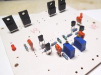
Fourth Picture:
Example routing/layout by member "Metallicus69" taken from #post490.
BYRTT, I always try to run high current away from my low current stuff. That is why I adopted that strategy. In my case it worked like a charm, but how does it work for others, I have no idea.
Cheers!
The main ground bus was a copper "pour", I removed it temporarily. With this software, it is easier to put those in last, because once the copper is laid it takes extra effort to move components around.That looks very much better.
Now repeat for lower half.
Then change the main (across the middle) ground link back to it's original width (where possible or waist it where not possible).
I would look at using a wire link to connect the measuring ground to the middle of the T between the two middle terminals of the output connectors.
If anyone makes a two sided board, then the wire link can be replaced with a top side trace.
If I am following your earlier comments correctly, then there are actually two different ground nodes left to connect. (C3, R3, R11) is one, and R9 is the other one, the one associated with the feedback node.
I am not sure what you mean by "measuring ground", but I assume that is R9, or what I have been calling feedback.
R9 can be rotated 90-degrees to put one end closer to the output ground terminals (C9 can be moved to make room for that, I just did not do it in the last post). If that is done, then there will be room for a separate trace to the output GND terminals.
The board is actually 2-sided w. plated holes now, but I want people to be able to etch it themselves if they want to. That was the point of the layout you first commented on. I have no objection to a few top layer traces.
You very kindly andBYRTT, I always try to run high current away from my low current stuff. That is why I adopted that strategy. In my case it worked like a charm, but how does it work for others, I have no idea.
Cheers!
 not impose anybody to doo if they want their own way (freedom), like that human behavour. HOW to learn this behavour to our political leaders who make rules for everything nowadays .
Getting the knowledge posted here is gold with freedom to choose. Last 3-4 years i have understand these post about such routing/layout rules and it is very audible in sentitive circuits, so why not use it also in less sensitive circuits with probably no downside.
Funny thing i have wondered after learning this is that i am very shure that in past i have judged diverse devices and circuits to be bad sounding in sensitive circuits, and probably it just sounded bad because of my horible routing/layout/lack of choice/knowledge
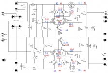
.The central circuit "measures" the voltage and determines the error at the output and sends a control signal to the pass device to adjust the output.
The measuring is of the voltage from Supply rail to Ground rail. That "measurement" should be taken at the output of the regulator/multiplier. It's this remote sensing (of the voltage at the output) that Salas talks about (whatever others may say).
The measuring is of the voltage from Supply rail to Ground rail. That "measurement" should be taken at the output of the regulator/multiplier. It's this remote sensing (of the voltage at the output) that Salas talks about (whatever others may say).
How high can I go with the voltage while building only one polarity?
I found MOSFET IRFB4410 with 100V 96A and 8mOHM. I understand this Vds was the main limitation.
With my trafo I get around 82V DC unloaded. The lower power MOSFETS will see approx 50V while the JFET CCS the rest of 30V (this can be easily cured with a series dropping resistor). I am not sure if I am still within safe limits and/or if my math is right.
Cheers!
I think the mosfets will see almost the full unfiltered supply voltage drop, for a short time after power is turned on (same as the pass transistor).How high can I go with the voltage while building only one polarity?
I found MOSFET IRFB4410 with 100V 96A and 8mOHM. I understand this Vds was the main limitation.
With my trafo I get around 82V DC unloaded. The lower power MOSFETS will see approx 50V while the JFET CCS the rest of 30V (this can be easily cured with a series dropping resistor). I am not sure if I am still within safe limits and/or if my math is right.
Cheers!
The unfiltered voltage at the cap multiplier input rises quickly on power up, while the voltage at the RC filter rises slowly. In general this is a good thing, because it gives the Cap Multiplier inherent soft start characteristics. But, it means that the mosfets and the pass transistor see the full voltage, at least for a short time.
Hi.
I did supply the following elements:
BYW29-200
BS170, BS250
IRF9540, IRF540.
Capacitors 6800UF the bridge and 1000uF output. Without the output capacitor arrangement strongly attracted.
I did supply the following elements:
BYW29-200
BS170, BS250
IRF9540, IRF540.
Capacitors 6800UF the bridge and 1000uF output. Without the output capacitor arrangement strongly attracted.
Attachments
Hi Pete,
I have assembled a new CP using the parts you listed below except I used MUR860G for the diodes. For some reason, I can't seem to get it to adjust the voltage. Are there some resistor changes that need to be made as well?
Thanks, Terry
I have assembled a new CP using the parts you listed below except I used MUR860G for the diodes. For some reason, I can't seem to get it to adjust the voltage. Are there some resistor changes that need to be made as well?
Thanks, Terry
PMI said:Terry,
Were you interested in a higher voltage Cap Multiplier?
This is a summary of the parts I plan to use to get there:
Rectifier diode: MSR860/MSRF860 (300V reverse voltage)
Pass Transistors: IRF5210PBF/IRF3710PBF (up to 100V)
BJT: KSC1845/KSA992 (120V)
Mosfets: ZVN3310/ZVP3310 (up to 100V)
I have only tested with the MSRF860 so far, so any comments are welcome.
The jfet only sees 1/2 the output voltage, so the 35V-rated J112 is good for up to 70V. It can also be replaced with a 5.6V constant current diode to get over 70V.
Pete
On the last CM I built, I had to decrease 180k to 150k to be able to adjust properly the voltage drop on the positive side. But I used different MOSFET transistors, BS170/BS250, and I assumed the reason was that. Also, 2SA970/2SC2240 fro the mirrors, and IRF3205/IRF4905 for the pass transistors.
Probably it's a better idea to use 150K, because the adjusted position will be closer to the midpoint of the trimmer (R7 + 1/2*VR1=150k)
Probably it's a better idea to use 150K, because the adjusted position will be closer to the midpoint of the trimmer (R7 + 1/2*VR1=150k)
Current is limited only by the pass transistor (and its heatsinking arrangements), but the pass transistor, LTP MOSFETs and input/output capacitors all need to withstand the full rail voltage. The RC filter and feeback capacitors see 0.5x the rail voltage. The JFET sees 1.5x the rail voltage in my design, or only 0.5x in PMI's. And don't forget the diodes.Is the pass mosfet the only item that restricts voltage and current delivery?
I mean what if one was to use a 250 volt part? Could we run an 80 volt supply?
You may also need to change the values of the feedback resistors, since the dropout voltage changes with input voltage, and the available range of adjustment will be exceeded at some point.
Ok, I finally had a some time to sit down and take some measurements. Please see attachment. The blue numbers represent the working unit and the red numbers represent the non working one. the working one uses IRF5305/IRLZ34N, BC556B/BC546B, ZVN2106A/ZVP2106A. The non working uses IRF5210PBF/IRF3710PBF, KSC1845/KSA992, ZVN3310/ZVP3310. Something is not working right but I don't understand enough to figure it out. Suggestions welcome.
Thanks, Terry
Thanks, Terry
Attachments
The thing that stands out about those measurements is the voltage at the bases of the current mirror transistors. It shouldn't be possible for them to be more than 0.6V from the rails. After seeing that, I checked the datasheet for KSA992, and the pinout is ECB, whereas the BC5x6 are CBE. You might be able to bend the leads enough to get them in the right way.
Those devices comprise the current mirror for the differential amplifier and actually are not exposed to much voltage across them. The limiting devices are the pass transistors (they see full voltage across them during start-up) and secondarily the differential amplifier MOSFETs and current source JFETs, which in PMI's version see about half a rail.
The BC546 / BC556 pair are 65Vce devices and aren't likely to see more than the required gate voltage of the pass transistor so should work with virtually any rail voltage.
The BC546 / BC556 pair are 65Vce devices and aren't likely to see more than the required gate voltage of the pass transistor so should work with virtually any rail voltage.
- Status
- This old topic is closed. If you want to reopen this topic, contact a moderator using the "Report Post" button.
- Home
- Amplifiers
- Power Supplies
- Finished capacitance multiplier