As such all these components are picking up interference that can easily be avoided by improving the layout.
Yes, but the question is how much interference is picked? If it is very little, almost negligible, than there will be no cosequences. There is no way that real world pcb will not pick some and we are dealing with amateur audio circuits here, not with high tech lab instruments. But of course, if it is possible to improve pcb in easy way, it should be done.
Sorry, misunderstood the question.I think I was basically asking if I understoon one line in your comments, correctly (?)
Yes, the same as I suggested and became adopted for the Salas regulators. He called it remote sensing.
This is a bit like the Kelvin Connections (?, not sure of name) as per Salas's shunt regs, for example, and others - ie get the 'sense' cct components off any track, thick or not, that carries power, dirty current 'bits' etc and simplify the current circuits ....
So, one track that goes directly from the Central 0 volt point to the transformer centre tap, and possibly includes the primary smoothing caps C1 & C5, then a separate short track to the output cap C9, and you could possibly group up the R9, R11, Q11 and even include the R3, C3 as well or another separate track, and this one is short/close to the central 0v, as Andrew mentioned.
I think you did this earlier, or the separating the Transformer and filter cap ground track at least, with no discernible improvement, but the smaller component relocation might be worth looking at in any later pcb review.
I cut a few tracks and ran separate wires on a few of these but didn't notice anything 'big' in the way of changed sound but when I changed the o/p caps and added some secondary R-C filters, there was a change in the sound (here, it's pick your own flavour kind of thing!)
Pete, on your second set of boards and components (thanks for those, by the way!) I put the schottky diodes, R-C snubbers, and the C-R-C externally to the main pcb with a separate 0volt line to the central 0v point and got a noticeable difference in the bass/low mids on the F5 amp, but it's a fair bit of extra effort for 'small beer' return, IMO (and this is from a 'clean bass nutter' like me!)
I'm a bit cynical when it comes to ground plane layers and such things (reduce the radiated energy first approach) but I'm a bit surprised that someone hasn't chimed in here about the benefits, &/or problems.
Oh yes, my 0volt point (central 0v) does go to a 'floating ground 10R thermistor' in typical Pass fashion - no problems so far, in 25 years!
... my 2 cents
Yes, that was what I wanted to know.Sorry, misunderstood the question.
Yes, the same as I suggested and became adopted for the Salas regulators. He called it remote sensing.
No, I did not try that, or actually think of it. Did not even know it was called remote sensing.
That would be similar to how it works on some closely regulated non-audio PSUs where the load regulation is very important. Here, the output is supposed to be filtered, but the absolute voltage level will rise and fall with the load... allowing it to rise and fall helps to make it such a neat circuit, because the voltage drop across the pass transistor can stay very small. When the power supply gets hammered during heavy bass passages, the voltage at the reservoir caps drops, but the voltage on both sides of the pass transistor moves with it.
the multiple ground leads "read" a voltage. If these multiple ground points are at different voltages the "amplifier" in the middle of your circuit will change it's "output" to suits the differring voltages.
Note particularly C3. It shares a ground trace with components that send very non constant CURRENTs to the zero volts line.
Those varying currents will vary the voltage drop along that shared trace.
The effect is that interference will vary the voltage reference seen by C3. It will affect the amplifier and that will affect the output.
It's the same where the other "measuring" components are tied into a ground trace that is shared with other non constant current producers.
Remote sensing is not the best way to call it. Remote sense is when you take NFB point from loudspeaker terminal with separate wire to amp. There is much about it in some Serbian DIY forums. There are several project currently using it. The idea for it is inspired by lab measuring equipment.
Yes, you and I exchanged some notes on that, same subject.I think you did this earlier, or the separating the Transformer and filter cap ground track at least, with no discernible improvement, but the smaller component relocation might be worth looking at in any later pcb review.
The choice of output cap probably makes the most difference, but it depends on the amplifier. Not so much for VSSA, there are separate 1000 uFd FG-series caps on each rail, an RC, plus 10uFd film caps, so in that case the output caps are well "buffered" on each board. In other cases, the output cap may be much more important....when I changed the o/p caps and added some secondary R-C filters, there was a change in the sound (here, it's pick your own flavour kind of thing!)
The board was designed so it can be used as a filter only, using the DC+/- connections and the center ground connection. Did you see how Metallicus used the filter circuit, Post 499? I really like that, and someone else has already suggested making a board with two parallel filters, and no rectifier/reservoir cap.Pete, on your second set of boards and components (thanks for those, by the way!) I put the schottky diodes, R-C snubbers, and the C-R-C externally to the main pcb...
No sure I understand that, sorry...Oh yes, my 0volt point (central 0v) does go to a 'floating ground 10R thermistor' in typical Pass fashion - no problems so far, in 25 years! ...

not only.Remote sensing is not the best way to call it. Remote sense is when you take NFB point from loudspeaker terminal with separate wire to amp. There is much about it in some Serbian DIY forums. There are several project currently using it. The idea for it is inspired by lab measuring equipment.
In this case the "measuring" reference is being taken to the output ground. It goes nowhere near the amplifiers load.
As shown "it" is being taken to several points spread between the input ground and the output ground.
Yes, C3 can be separated from C5 and R13 fairly easily. The central ground bus is fairly clean, to the best of my ability to test. It is actually a pretty low impedance path, when you consider the size.... Note particularly C3. It shares a ground trace with components that send very non constant CURRENTs to the zero volts line.
Those varying currents will vary the voltage drop along that shared trace.
The effect is that interference will vary the voltage reference seen by C3. It will affect the amplifier and that will affect the output...
If I separate the components in the filter circuit from the main ground bus (which is how it was in the beginning), I will also separate the ground reference for the two rails from each other. Based on past experience, that was something I wanted to avoid, but perhaps this is a case where the top layer can and should be used....

...I'm a bit cynical when it comes to ground plane layers and such things (reduce the radiated energy first approach) but I'm a bit surprised that someone hasn't chimed in here about the benefits, &/or problems...
If I were to design a 2-layer PCB for this, I would make the top layer a ground plane. Not so much because of the electrical benefits, but because every bit of copper etched is money wasted, so you might as well try to fill every layer as much as possible....If I separate the components in the filter circuit from the main ground bus (which is how it was in the beginning), I will also separate the ground reference for the two rails from each other. Based on past experience, that was something I wanted to avoid, but perhaps this is a case where the top layer can and should be used....
If I were to design a single layer PCB, then I would go with star grounding (local star ground on the PCB, plus the main star ground attached to the chassis)... which is what I actually did of course. I never did any measurements to see if it had a real benefit, but there is no downside.
Attachments
you take NFB point from loudspeaker terminal with separate wire to amp. There is much about it in some Serbian DIY forums. There are several project currently using it.
Are they doing something similar to Kenwood's Sigma Drive?
Are they doing something similar to Kenwood's Sigma Drive?
I don't know if it is similar to Kenwood's Sigma Drive, but I would not be surprised if it is. The idea is, if I understand it, to eliminate distortions and anomalies present in loudspeaker cables simultaneously with amp distortions.
How do you keep that feedback wire free of EMI/RFI and any other interference, shielded cable?I don't know if it is similar to Kenwood's Sigma Drive, but I would not be surprised if it is. The idea is, if I understand it, to eliminate distortions and anomalies present in loudspeaker cables simultaneously with amp distortions.
How do you keep that feedback wire free of EMI/RFI and any other interference, shielded cable?
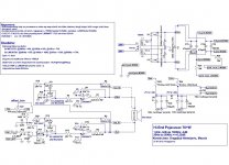
To be honest I do not follow those threads seriously (because these threads are epic in length) and do not know the answer to your question. I would have to read some of it to see. Here you have schematic of one such amp designed by the legendary Dragoljub Aleksijević - Macola that uses LM3886 power ICs.
Attachments
I'm not sure that you would need to do much. For instance ATX power supplies use a simple unshielded wire for 3.3V remote sensing. While the wire is not very long compared to a speaker cable, the inside of a PC is full of RF. This might be a good use of a spare pair in a Cat5 cable.How do you keep that feedback wire free of EMI/RFI and any other interference, shielded cable?
Pete i have 4 of our nice PCBs and will use when i get there, thanks for that (lots of good reviews from members so look forward), and documented measurements are top class.
For routing/layout concerns started by member "AndrewT" i have little input. First i say that nothing of my input is to make shipped PCB's better without documented measurements or listening tests. It is what i have learned from this site and books and i only post for getting knowledge out and feedback back so everybody can learn. Think it is same boat as members "AndrewT" and "Jameshillj" mention. This routing/layout are very audible in sensitive preamps for audio/musical instrument, and best it is no cost in bits and pieces.
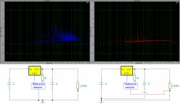
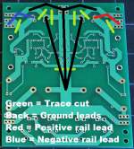
First Picture:
LM317 example with same schematic but different routing/layout. In a simulating program this will give same result but real world as seen is very different. The plots i downloaded somewhere from this site couble of years ago and as i remember was taken with 16bit soundcard. The schematic layout underneath i made myself tonight before posting for understanding of routing seen in plots.
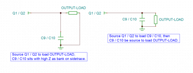
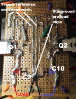
Second Picture:
Taking on SMALL shoes, little routing improvement can be made for C9/C10, see text in Picture.
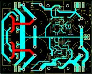
Third Picture:
Example of one (or make your own) easy way to amend PCB for maybe better routing.
Fourth Picture:
Example routing/layout by member "Metallicus69" taken from #post490.
For routing/layout concerns started by member "AndrewT" i have little input. First i say that nothing of my input is to make shipped PCB's better without documented measurements or listening tests. It is what i have learned from this site and books and i only post for getting knowledge out and feedback back so everybody can learn. Think it is same boat as members "AndrewT" and "Jameshillj" mention. This routing/layout are very audible in sensitive preamps for audio/musical instrument, and best it is no cost in bits and pieces.
First Picture:
LM317 example with same schematic but different routing/layout. In a simulating program this will give same result but real world as seen is very different. The plots i downloaded somewhere from this site couble of years ago and as i remember was taken with 16bit soundcard. The schematic layout underneath i made myself tonight before posting for understanding of routing seen in plots.
Second Picture:
Taking on SMALL shoes, little routing improvement can be made for C9/C10, see text in Picture.
Third Picture:
Example of one (or make your own) easy way to amend PCB for maybe better routing.
Fourth Picture:
Example routing/layout by member "Metallicus69" taken from #post490.
Attachments
YES !!!!!Now I know why my LM317/337 regulator for phono stage has some noise (BYRTT first picture)............ do we still need adjustment pin ground to be connected at the load?
At the load connection, i.e the output side.
Last edited:
With regard to the discussion a couple pages back, here is another possible component placement. (The current one was really aiming at a different ground scheme, so, not so easily converted)R11 connect direct to Q11 source.
C3 to R3
R9 to Q11 trace
R3 to Q11 trace
Q11 trace to output, AT THE OUTPUT.
...
R11 relocated and connected directly to Q11 source
C3 relocated and connected to the junction of R1 and R3
R9 and VR1 relocated to make more room for R9 ground connection
R3 and R11 moved to allow common connection
The different filter nodes connected to ground are left unrouted and highlighted.
Attachments
That looks very much better.
Now repeat for lower half.
Then change the main (across the middle) ground link back to it's original width (where possible or waist it where not possible).
I would look at using a wire link to connect the measuring ground to the middle of the T between the two middle terminals of the output connectors.
If anyone makes a two sided board, then the wire link can be replaced with a top side trace.
- Status
- This old topic is closed. If you want to reopen this topic, contact a moderator using the "Report Post" button.
- Home
- Amplifiers
- Power Supplies
- Finished capacitance multiplier