when you feel 55C - turn fans on , when you feel colder amp (colder days) , don't power them
that's not nuclear science
ZM, the temperature in the room where this amplifier will be operating will be the same year-round, always 74 - 76 degrees F. It will not experience hot and cold days.

6L6,
Thanks for that link to ZM's cooling system! I had heard through the gravevine of their existence, but had not found the link. I will read through it tonight.
Good point on the fact that the turbos had no limiter circuit.
Toxic--great thread....thanks!
If you are still considering other cooling approaches, you might want to review my old F5 build thread:
http://www.diyaudio.com/forums/pass...erent-drummer.html?highlight=f5+drummer+music
A quick recap of the above thread: Two fans mounted vertically on the rear chassis apron. Air flowing into the "main chamber" of the amp, for component cooling, then under the heatsink lower surface, and the up between the heatsink fins and the wooden sides of the amp enclosure. This has proven to be very effective. I'll probably use this same chassis design for a large F5 turbo build.
Again, great thread..... thanks...........
Major setback, and still not sure what happened.
I had built a new cooling stand with fans on each side, 120 mm each, per ZM's suggestion, and the amplifier was sitting on the stand. The fans in the stand are not powered by the amplifier. I had inputs shorted and no load on speakers. The amp was biased at 0.8 A with relatively low temperatures - at least the heat sinks were not hot by any means.
After about 3.5 hours, having carefully rechecked bias and offset about 90 minutes earlier, and with heat sinks still warm, but not hot, I just happened to be standing near the amp with I heard a tiny "pffffst" for a fraction of a second and saw a tiny puff of smoke rise from the left amp board. The top panel was on the amp, so I couldn't see exactly where it came from, but the puff of smoke rose near the P-channel end of the board. I immediately turned off power, but a fuse had already blown (good). No probes were connected to the amplifier at this time and I was not touching the amp.
I examined both amp boards and the PS boards carefully and could see nothing wrong at all. I replaced a fuse and powered up with the light bulb in series and it glowed brightly. I disconnected both amp boards, and the bulb glowed brightly and then immediately dimmed, as the caps charged. With no amp boards connected, power supply voltages were perfect. So, PS OK.
If I connected either amplifier board, alone, the bulb glowed brightly. Seemed strange that something would happen to both sides of the amp at once, especially with dual mono power supplies. So I began collecting data on one side at a time.
LEFT SIDE
With only left transformer, left PS board and left amp amp board connected, the bulb shined brightly and I had 2.4 V (not mV) offset on the speaker terminals (it had been about 1.6 mV two hours earlier). Powered down and disconnected the L board. Set P1 and P2 to minimal resistance. Without removing components from the board, both P channel MOSFETs read zero ohms between drain and source. Both N channel MOSFETs read 260 ohms between drain and source, but were inconsistent between gates and drains (infinity and 200 ohms). 3 of 4 gate stoppers also read low (not open, but < 2 ohms), while one read 47 ohms. No shorts between any MOSFET lead and the heat sink. All source resistors, in circuit, read 0.5 ohms.
I removed the board and confirmed the above findings on the bench. Resistance readings on the JFETs, in circuit, show infinite resistance between drain and source on the 2SK174 and 36 ohms between drain and source on the 2SJ74, regardless of which lead was on the drain or on the source.
So, at least for the left board, I am going to change out all the MOSFETs and check gate stoppers with one lead out of circuit and may replace some of those, as well.
1. Would you also replace the JFETs, or should I remove them first and retest them? I have other matched pairs. Would it be wisest to replace them, regardless of what they read out of circuit?
RIGHT SIDE
With the left board out of the amplifier, I powered up only the right transformer, right PS board, and R amp board. The bulb glowed bright, but I had no voltage drop across MOSFET source resistors (I was measuring on N-channel MOSFETs) and had speaker offset of about 5 mV (that could have been stray readings on the volt meter). I set P1 and P2 to minimal resistance, and the bulb went dim. I gradually increased resistance on P1 and P2, and the bulb would glow brightly, but I could not measure a voltage drop across source resistors on a MOSFET, but only checkrf one on an N channel device. I hope I am not going insane. I'll get to that board after fixing the left side first, but am open to any suggestions or insights about the right board or about what may have caused both sides to fail at once.
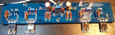
I'll put the scope on the PS boards in the next day or two, as well. I attached a photo of the L board, and can take detailed close-ups, but everything looks fine, even under the magnifying glass. The underside also looks fine.
Thanks.
I had built a new cooling stand with fans on each side, 120 mm each, per ZM's suggestion, and the amplifier was sitting on the stand. The fans in the stand are not powered by the amplifier. I had inputs shorted and no load on speakers. The amp was biased at 0.8 A with relatively low temperatures - at least the heat sinks were not hot by any means.
After about 3.5 hours, having carefully rechecked bias and offset about 90 minutes earlier, and with heat sinks still warm, but not hot, I just happened to be standing near the amp with I heard a tiny "pffffst" for a fraction of a second and saw a tiny puff of smoke rise from the left amp board. The top panel was on the amp, so I couldn't see exactly where it came from, but the puff of smoke rose near the P-channel end of the board. I immediately turned off power, but a fuse had already blown (good). No probes were connected to the amplifier at this time and I was not touching the amp.
I examined both amp boards and the PS boards carefully and could see nothing wrong at all. I replaced a fuse and powered up with the light bulb in series and it glowed brightly. I disconnected both amp boards, and the bulb glowed brightly and then immediately dimmed, as the caps charged. With no amp boards connected, power supply voltages were perfect. So, PS OK.
If I connected either amplifier board, alone, the bulb glowed brightly. Seemed strange that something would happen to both sides of the amp at once, especially with dual mono power supplies. So I began collecting data on one side at a time.
LEFT SIDE
With only left transformer, left PS board and left amp amp board connected, the bulb shined brightly and I had 2.4 V (not mV) offset on the speaker terminals (it had been about 1.6 mV two hours earlier). Powered down and disconnected the L board. Set P1 and P2 to minimal resistance. Without removing components from the board, both P channel MOSFETs read zero ohms between drain and source. Both N channel MOSFETs read 260 ohms between drain and source, but were inconsistent between gates and drains (infinity and 200 ohms). 3 of 4 gate stoppers also read low (not open, but < 2 ohms), while one read 47 ohms. No shorts between any MOSFET lead and the heat sink. All source resistors, in circuit, read 0.5 ohms.
I removed the board and confirmed the above findings on the bench. Resistance readings on the JFETs, in circuit, show infinite resistance between drain and source on the 2SK174 and 36 ohms between drain and source on the 2SJ74, regardless of which lead was on the drain or on the source.
So, at least for the left board, I am going to change out all the MOSFETs and check gate stoppers with one lead out of circuit and may replace some of those, as well.
1. Would you also replace the JFETs, or should I remove them first and retest them? I have other matched pairs. Would it be wisest to replace them, regardless of what they read out of circuit?
RIGHT SIDE
With the left board out of the amplifier, I powered up only the right transformer, right PS board, and R amp board. The bulb glowed bright, but I had no voltage drop across MOSFET source resistors (I was measuring on N-channel MOSFETs) and had speaker offset of about 5 mV (that could have been stray readings on the volt meter). I set P1 and P2 to minimal resistance, and the bulb went dim. I gradually increased resistance on P1 and P2, and the bulb would glow brightly, but I could not measure a voltage drop across source resistors on a MOSFET, but only checkrf one on an N channel device. I hope I am not going insane. I'll get to that board after fixing the left side first, but am open to any suggestions or insights about the right board or about what may have caused both sides to fail at once.
I'll put the scope on the PS boards in the next day or two, as well. I attached a photo of the L board, and can take detailed close-ups, but everything looks fine, even under the magnifying glass. The underside also looks fine.
Thanks.
Attachments
Last edited:
there is no other xplanation than inconsistent mosfet mounting on heatsink (either pressure or metal splinter residue
pull all semis out and retest
Thanks, Zen.
Removed both boards and removed all semiconductors this afternoon. I also removed the mica insulators and thermal compound from the sinks. I closely inspected all boards and tested each transistor.
Left Channel
1 P-channel MOSFET tests good with multimeter diode test (and appropriate switching on with charge to gate, and switching off with gate to source, etc.).
1 P-channel MOSFET is shorted.
2 N-channel MOSFETs are shorted.
All gate-stoppers test exactly 47 ohms.
All source resistors test normally.
Both bipolars test normal with diode tester.
Both JFETs test normal with ohm meter, and give identical values to those of new JFETs I compared them to.
Right Channel
All MOSFETs test good with diode test on multimeter and switching on and off, etc.
All gate-stoppers test exactly 47 ohms.
All source resistors test normally.
Both bipolars (cascoders) test normal with diode tester.
Both JFETS test normal, as described above and when compared to new ones.
All MOSFETs were firmly and equally secured to the heat sink. Again, there were no shorts from any MOSFET lead to the heat sinks before removing the boards.
I am blowing out the chassis to get rid of any hidden tiny metal flakes or dust or wire whiskers, and will wipe down the entire inside with a tack cloth to pick up any dust, etc. I have inspected each amp board closely and can see no shorts of any kind from flakes of metal, whiskers of wire, etc, but have also cleaned the boards.
Certainly, I will replace all MOSFETs on the left board.
1. Should I trust my JFET test, or should I simply replace the left board JFETs?
2. I plan to reuse the bipolars on the left. Any problem with this?
On the right board, the MOSFETs test normal, but I have extra.
3. Should I simply replace the MOSFETs on the right side and remove any possibility of a problem with them?
4. How about JFETs on the right? I have extra.
I still am unclear about the behavior of the right board, even though MOSFETs and JEFETs have tested normal. This is why I lean towards simply replacing them.
Of note, your comment about metal particles/dust/whiskers is compatible with the fact that I had moved and tilted the amplifier before placing it on the new cooling pad. But, again, the amp ran fine for 3 hours before the sudden failure.
Thanks.
you can fire up the jfets without the Mosfets in, or with the drive resistors not connected... you ought to see the right bias points come up... also they will pass signal as seen with a scope.
Replacing is simple too...
regarding the cooling... my suggestion is/was to make the platform sealed on at least 3 sides, foam was one way, this will permit more or less a pressurized compartment between the fan exit and the bottom of the chassis. This will force air through the bottom panel just fine, regardless of where the fan is positioned.
_-_-
Hi Bear,
I had plenty of matched semis. I just changed out all the MOSFETs and JFETs to remove any questions, but reused the cascoding transistors. Didn't take too long. I'll get the boards back on the heat sinks and biased up today sometime.
I used compressed air to clean out the chassis and will wipe everything down with a tack cloth before reassembly. Also will take a look at PS outputs on the scope, but don't anticipate it is likely to find an issue.
The current fan locations appear to be fine, and I'll post a photo later. The foam option for creating a seal between the bottom of the amp and the cooling board, on first impression, makes me a bit nervous - I would think air flow could be impaired in the event of a fan failure, which would not necessarily be recognized.
Steve
The temporary setback is resolved. After removing boards and replacing JFETs and MOSFETs, I blew out the amplifier with compressed air and then wiped down every surface, crack, transformer, capacitor, etc. with a tack cloth to pick up any particles of dust, metal, etc.
I remounted the boards and the amplifier biased up just fine. After letting it set for a couple hours biased at 0.8 A, I again adjusted P3 on both boards using the distortion analyzer and the scope with FFT on the residual waveform. Both channels ended up below 0.004% THD at 1 watt output, 1 kHz. One P3 did not require adjustment, as it was already at the minimal THD and had a minimal 3rd harmonic. The other channel had a strong 3rd, and adjustment of P3 dropped THD from about 0.0065% to less than 0.004% with almost disappearance of the 3rd on the FFT. (Of course, the FFT on the residual is, again, only used to examine the relative strength of 2nd versus 3rd harmonic and cannot detect something as low as -80 or -70 dB.)
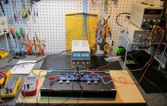
All of these were done with the amplifier sitting on the new cooling stand with dual fans, as suggested by Zen Mod. These are 5VDC fans with 50 ohm resistance, each, wired in parallel. The stand is 16 inches wide, 14 inches deep, and 1 inch thick with feet that are 7/8 inch tall. When operating, not only did air move into the amplifier, but I could feel some cool air coming up the sides of the amp (on the outside) across the heat sinks. A pleasant surprise. I grabbed a 25 ohm, 3 W rheostat and found that at 4 volts, cooling was still good, but fan noise all but disappeared adjacent to the amplifier. Thus, I will replace the rheostat with about a 5 or 6 ohm resistor in a small enclosure with a switch that will allow operation at 4 or 5 volts.
Biased at 0.8A, sitting on the cooling stand with fans running at 4 volts, and music playing loudly (just beyond class A) temperature measurements showed:
Heat sink top about 47 C.
Heat sink next to MOSFETs about 55 C
MOSFET source resistors about 52 C
JFETs about 51 C
MOSFET pin 2 about 68 to 70 C.
Everyone, thanks so much for all the essential assistance you have provided in this build. I now must sit back and consider my next projects, but I am leaning towards some speakers.
Steve
I remounted the boards and the amplifier biased up just fine. After letting it set for a couple hours biased at 0.8 A, I again adjusted P3 on both boards using the distortion analyzer and the scope with FFT on the residual waveform. Both channels ended up below 0.004% THD at 1 watt output, 1 kHz. One P3 did not require adjustment, as it was already at the minimal THD and had a minimal 3rd harmonic. The other channel had a strong 3rd, and adjustment of P3 dropped THD from about 0.0065% to less than 0.004% with almost disappearance of the 3rd on the FFT. (Of course, the FFT on the residual is, again, only used to examine the relative strength of 2nd versus 3rd harmonic and cannot detect something as low as -80 or -70 dB.)
All of these were done with the amplifier sitting on the new cooling stand with dual fans, as suggested by Zen Mod. These are 5VDC fans with 50 ohm resistance, each, wired in parallel. The stand is 16 inches wide, 14 inches deep, and 1 inch thick with feet that are 7/8 inch tall. When operating, not only did air move into the amplifier, but I could feel some cool air coming up the sides of the amp (on the outside) across the heat sinks. A pleasant surprise. I grabbed a 25 ohm, 3 W rheostat and found that at 4 volts, cooling was still good, but fan noise all but disappeared adjacent to the amplifier. Thus, I will replace the rheostat with about a 5 or 6 ohm resistor in a small enclosure with a switch that will allow operation at 4 or 5 volts.
Biased at 0.8A, sitting on the cooling stand with fans running at 4 volts, and music playing loudly (just beyond class A) temperature measurements showed:
Heat sink top about 47 C.
Heat sink next to MOSFETs about 55 C
MOSFET source resistors about 52 C
JFETs about 51 C
MOSFET pin 2 about 68 to 70 C.
Everyone, thanks so much for all the essential assistance you have provided in this build. I now must sit back and consider my next projects, but I am leaning towards some speakers.
Steve
Attachments
Last edited:

Please pm me if you are interested.
Private messaging to you seems to be disabled. I would like to purchase a pair of boards.
MOSFET Shorted Again – Oscillation?
Back in post #104, and as described in the posts that followed it, 3 of 4 MOSFETs in the left channel had suddenly shorted. Zen suggested inconsistent MOSFET mounting or splinter residue. On replacing components, the MOSFETs seemed to be mounted just fine, there were no shorts between the MOSFETs and the heat sinks, and I didn’t see any obvious evidence of splinters or metal dust (from drilling).
Regardless, as described earlier in this thread, I replaced JFETs and MOSFETs in both boards and completely blew out and wiped down he entire amp. Everything appeared to be going well, and the amplifier sounded incredible and ran without problems for a several weeks. I then took it to a friend in another city. There it was installed on a home theater system. It received input from a preamp and was used to power front 8 ohm speakers. Sounded great and ran without problems for a few weeks.
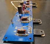
Last week, while visiting to recheck bias a final time after about 4 weeks of use, I had the speakers attached and input cables attached from the preamp. The F5 was on, but the preamp was off. That is, no signal coming in and no output to speakers. I removed the input cable (RCA plug) to the R channel and there was a sudden puff of smoke from the R board instantly, and the fuse blew.
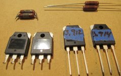
On inspection, as shown in the first photo, the source resistors (2 one-ohm 5 watt resistors in parallel) were discolored adjacent to the N-channel device on the end of the board, and the device was shorted between all leads. Other MOSFETs tested fine. I removed the board and the amplifier powered up fine with the L channel in place. I brought the board home with me for repairs.
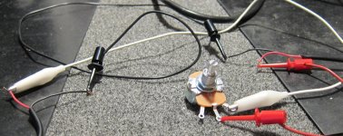
I removed both N-channel devices and the source resistors on the end device. Only the MOSFET on the end was shorted and all source resistors, including the discolored ones, tested normal, but I chose to replace the dicolored ones, of course. I had a new matched N-channel MOSFETs as shown in the second photo.
Gatestoppers all tested fine (photo).
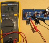
I installed the board on an extra heat sink I had and powered it up to between 5 and 22 V rails to be sure it would bias without shorts, and it behaved normally (photo).
So….what had happened? Bear pointed out that while the amplifier should be stable, some amps in the past have been famous for parasitic oscillation when cables are added or removed while powered up, and wondered if oscillation might be the case here. I had been afraid to mention the possiblity, but had wondered whether parasitic oscillation could have explained the first MOSFET failure given I saw no evidence for poor mounting or splinters. Again, I (we) didn’t know if oscillation was occurring, but I certainly took the possibility seriously. At higher rail voltages with 4 N-channel devices and 4 P-channel devices (and diodes) in the turbo V3, Nelson noted that he could detect some ringing at times and included an optional compensation cap between the output (drains) and just before the gatestoppers for the MOSFETs (one cap per board). These caps were found to be necessary for builds by, for example, 6L6. And various postings over the years have described increasing stability by increasing the resistance of the gatestoppers. 6L6 kindly reminded me that the cap in the version 3 turbo is 1 nF and the gatestoppers could be increased up to 680R (from 47R at present) without a significant change in sound. Bear provided some clear guidance on examining the amplifier with sine, triangle, and square waves to seek evidence of ringing, and noted that compensation caps smaller than 1 nF were commonly effective. I had put plenty of sine waves through the amp during the build, well into clipping, but had not examined triangle waves or square waves in much detail.
This weekend I hopped on a plane with the repaired board, a digital scope (trying to travel light), signal generator, power resistors, extra parts, 1 nF film caps, 680R resistors, meters, etc., and went to reinstall the board and examine the amplifier in more detail. I only lost a single needle-nosed pliers to the TSA agents (it was 7.5 inches long - measured with a ruler by the agent - and any "tool" over 7 inches must be confiscated.) No kidding. 7 inch pliers are harmless. 7.5 inch pliers are a threat.)
Back in post #104, and as described in the posts that followed it, 3 of 4 MOSFETs in the left channel had suddenly shorted. Zen suggested inconsistent MOSFET mounting or splinter residue. On replacing components, the MOSFETs seemed to be mounted just fine, there were no shorts between the MOSFETs and the heat sinks, and I didn’t see any obvious evidence of splinters or metal dust (from drilling).
Regardless, as described earlier in this thread, I replaced JFETs and MOSFETs in both boards and completely blew out and wiped down he entire amp. Everything appeared to be going well, and the amplifier sounded incredible and ran without problems for a several weeks. I then took it to a friend in another city. There it was installed on a home theater system. It received input from a preamp and was used to power front 8 ohm speakers. Sounded great and ran without problems for a few weeks.
Last week, while visiting to recheck bias a final time after about 4 weeks of use, I had the speakers attached and input cables attached from the preamp. The F5 was on, but the preamp was off. That is, no signal coming in and no output to speakers. I removed the input cable (RCA plug) to the R channel and there was a sudden puff of smoke from the R board instantly, and the fuse blew.
On inspection, as shown in the first photo, the source resistors (2 one-ohm 5 watt resistors in parallel) were discolored adjacent to the N-channel device on the end of the board, and the device was shorted between all leads. Other MOSFETs tested fine. I removed the board and the amplifier powered up fine with the L channel in place. I brought the board home with me for repairs.
I removed both N-channel devices and the source resistors on the end device. Only the MOSFET on the end was shorted and all source resistors, including the discolored ones, tested normal, but I chose to replace the dicolored ones, of course. I had a new matched N-channel MOSFETs as shown in the second photo.
Gatestoppers all tested fine (photo).
I installed the board on an extra heat sink I had and powered it up to between 5 and 22 V rails to be sure it would bias without shorts, and it behaved normally (photo).
So….what had happened? Bear pointed out that while the amplifier should be stable, some amps in the past have been famous for parasitic oscillation when cables are added or removed while powered up, and wondered if oscillation might be the case here. I had been afraid to mention the possiblity, but had wondered whether parasitic oscillation could have explained the first MOSFET failure given I saw no evidence for poor mounting or splinters. Again, I (we) didn’t know if oscillation was occurring, but I certainly took the possibility seriously. At higher rail voltages with 4 N-channel devices and 4 P-channel devices (and diodes) in the turbo V3, Nelson noted that he could detect some ringing at times and included an optional compensation cap between the output (drains) and just before the gatestoppers for the MOSFETs (one cap per board). These caps were found to be necessary for builds by, for example, 6L6. And various postings over the years have described increasing stability by increasing the resistance of the gatestoppers. 6L6 kindly reminded me that the cap in the version 3 turbo is 1 nF and the gatestoppers could be increased up to 680R (from 47R at present) without a significant change in sound. Bear provided some clear guidance on examining the amplifier with sine, triangle, and square waves to seek evidence of ringing, and noted that compensation caps smaller than 1 nF were commonly effective. I had put plenty of sine waves through the amp during the build, well into clipping, but had not examined triangle waves or square waves in much detail.
This weekend I hopped on a plane with the repaired board, a digital scope (trying to travel light), signal generator, power resistors, extra parts, 1 nF film caps, 680R resistors, meters, etc., and went to reinstall the board and examine the amplifier in more detail. I only lost a single needle-nosed pliers to the TSA agents (it was 7.5 inches long - measured with a ruler by the agent - and any "tool" over 7 inches must be confiscated.) No kidding. 7 inch pliers are harmless. 7.5 inch pliers are a threat.)
Attachments
- Status
- This old topic is closed. If you want to reopen this topic, contact a moderator using the "Report Post" button.
- Home
- Amplifiers
- Pass Labs
- F5c (cascode) cviller boards 40 V rails build