Hi Andrew. Please correct me if I am wrong.
There are two devices on each side of the push pull, and each device is biased to 0.8 A. That is, at bias, there is 1.6 A on each side of the push pull. 1.6A flowing through the N-channel MOSFETs and 1.6A flowing through the P-channel MOSFETs.
This amp, then, will remain in class A until 1.6 A X 2 = 3.2 A.
Peak power = 3.2A X 3.2A X 8R = 81.92 W.
Average power is 1/2 peak for a sine wave.
Average power = 81.92 W/2 = about 41 W.
This is wrong.Peak power = 3.2A X 3.2A X 8R = 81.92 W.
Your figure of 3.2A is actually 3.2Apk.
Forget about peak power.
Use the formula that applies: P = IV = V²/R = I²R
This applies to DC from where it originally came.
If the current and voltage are not constant value DC, then you MUST substitute Vrms for V and Irms for I
Vrms has the same heating power as a constant value of Vdc.
Irms has the same heating power as a constant value of Idc.
The formulae become:
P = IrmsVrms = Vrms²/R = Irms²R
When the signal is sinewave the exact same formulae apply.
But you can also use the peak values of the sinewave waveform.
Now the formula that apply to sinewave become:
P = IpkVpk/2 = Vpk²/R/2 = Ipk²R/2
No where does instantaneous peak power enter the discussion.
Reserve that for junction and component dissipation where a peak or instantaneous dissipation must be adhered to.
Do not use peak instantaneous power for the average power delivered by a stage, that heats a non reactive load.
Last edited:
Andrew, thanks for helping me out on this and being patient with me. My calculation is based on Nelson’s article on the F5. As you know, the original F5 has two MOSFETs rather than four, and they are biased to 1.3 A, each.
Nelson wrote:
For this sort of circuit, a 1.3 amp bias means that the amplifier will operate Class A to 2.6 amps of output current. To understand this, imagine a condition where Q3 and Q4 [the MOSFETs] are idling at 1.3 amps, so that all the current is going from the V+ voltage rail to the V- voltage rail, and none is going through the loudspeaker.
When a positive voltage appears at the Gates of Q1 and Q2, it makes the current through Q1 increase and the current through Q2 decrease. The resulting voltages across R3 and R4 make the current through Q3 increase and the current through Q4 decrease. This makes the output voltage go positive. As the positive input voltage increases, you approach the point at which Q3 is conducting 2.6 amps and Q4 is conducting 0 amps – and all of the 2.6 amps goes through the loudspeaker.
The power of 2.6 amps into 8 ohms is I^2 * R, or 2.6 * 2.6 * 8 = 54 watts. This is the peak value, and the nature of an undistorted sine wave is that the peak wattage is twice the average, so this circuit would operate 27 watts average Class A into 8 ohms. At currents above 2.6 amps one of the transistors will shut off, leaving the other to continue to increase beyond the 2.6 amps in what is known as Class AB.
Andrew, I assume you agree that my calculation was along the same rationale as that of Nelson, is that correct? That is, I start with 1.6 A rather than 1.3 A, but otherwise use the same sort of reasoning to end up with 41 W average power out.
Later today I will study your post and see if I can understand my error as this is something important for me to understand.
Thanks,
Steve
I continue to ask for advice and suggestions to help me accurately calculate average power out while in Class A. Is it really 41 W as I calculated?
But moving on in the interim, a major issue in building this amplifier has centered around heat generation and dissipation, as expected. Appropriate concerns and questions were raised regarding JFET temps, MOSFET source resistor temps, etc.
In post #42, I reported temperature measurements at 0.8 A bias with inputs shorted and no load on speakers after the top and front were on the amplifier for a few hours. I had measured:
MOSFET temperature (measured on the device) averaged 69.4 C ( 157 F).
MOSFET source resistors were also 69.4 C (157 F).
Heatsink temperature in proximity to MOSFETs was 60.5 C (141 F).
Heatsink temperature on top surface was about 50 C (122 F).
JFET temperatures averaged about 57.2 C (135 F).
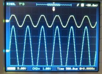
So I thought it important to see what temperature issues might result with the amplifier working maximally, while carefully monitoring temps and waveforms. I placed 8 ohm, 100 W power resistors (elevated on ceramic bases because they get HOT) on speaker terminals. I sent a sine wave into both channels to generate an amplifier output on both channels that was significantly clipped on both sides of the sine wave. The input sine wave was 3.4 V peak (not RMS). Output sine wave would be clipping, of course, at rail voltages. My attempt was to clearly exceed 80 W RMS output for a period of time. Again, I was carefully monitoring temperatures by intermittently lifting off the top and taking measurements while also watching the scope. At the wall the amplifier was drawing 4.2 A. (Photo attached.)
After 30 minutes, temperatures were as follows:
MOSFET device 56.1 C (133 F)
MOSFET source resistor 77.8 C (172 F)
Of course, a lot of power was heading out to the power resistors on the speaker terminals rather than to the heat sinks. I suspect MOSFET temperature would have risen some more if I kept going, but have a feeling the source resistors wouldn't have risen much. Even another 30 degrees F on the MOSFET would not have been a problem. But this was a 30 minute test.
I then simply sent the output from an ipod into the amp inputs and set the ipod on maximal volume and played music into 8 ohm speakers (rather than power resistors) at full ipod volume for 2 hours (not 30 minutes as was done in the first test) and again took measurements. I have never played a calibrated to dB sine wave at 1 kHz on an ipod, so I don’t know what the maximal output voltage is. As you know, wave forms are all over the place when monitoring music. Power out was less than in the clipping test, just described, but it sure was very loud. The amp was drawing 3.84 A at the wall indicating the amp was just beyond leaving class A (recall the amp used 3.7A at bias, no signal in, no speaker load). I simply wanted something that was realistic and real to life with how the amplifier would be used, though I recognize that a preamp and, I presume, a CD player can certainly generate a stronger output than an Ipod. The volume was significantly louder than I would listen to, however.
After 2 hours I took some random measurements:
MSOFET source resistor 62.2 C (144 F)
JFET 52.8 C (127 F)
Heat sink in proximity to MOSFET 62.2 C (140 F)
Ambient temp in middle of amp 44.4 C (112 F)
The heat sink temp of 140 F suggests a MOSFET temp of about 156 F or so, but I didn't measure it.
But moving on in the interim, a major issue in building this amplifier has centered around heat generation and dissipation, as expected. Appropriate concerns and questions were raised regarding JFET temps, MOSFET source resistor temps, etc.
In post #42, I reported temperature measurements at 0.8 A bias with inputs shorted and no load on speakers after the top and front were on the amplifier for a few hours. I had measured:
MOSFET temperature (measured on the device) averaged 69.4 C ( 157 F).
MOSFET source resistors were also 69.4 C (157 F).
Heatsink temperature in proximity to MOSFETs was 60.5 C (141 F).
Heatsink temperature on top surface was about 50 C (122 F).
JFET temperatures averaged about 57.2 C (135 F).
So I thought it important to see what temperature issues might result with the amplifier working maximally, while carefully monitoring temps and waveforms. I placed 8 ohm, 100 W power resistors (elevated on ceramic bases because they get HOT) on speaker terminals. I sent a sine wave into both channels to generate an amplifier output on both channels that was significantly clipped on both sides of the sine wave. The input sine wave was 3.4 V peak (not RMS). Output sine wave would be clipping, of course, at rail voltages. My attempt was to clearly exceed 80 W RMS output for a period of time. Again, I was carefully monitoring temperatures by intermittently lifting off the top and taking measurements while also watching the scope. At the wall the amplifier was drawing 4.2 A. (Photo attached.)
After 30 minutes, temperatures were as follows:
MOSFET device 56.1 C (133 F)
MOSFET source resistor 77.8 C (172 F)
Of course, a lot of power was heading out to the power resistors on the speaker terminals rather than to the heat sinks. I suspect MOSFET temperature would have risen some more if I kept going, but have a feeling the source resistors wouldn't have risen much. Even another 30 degrees F on the MOSFET would not have been a problem. But this was a 30 minute test.
I then simply sent the output from an ipod into the amp inputs and set the ipod on maximal volume and played music into 8 ohm speakers (rather than power resistors) at full ipod volume for 2 hours (not 30 minutes as was done in the first test) and again took measurements. I have never played a calibrated to dB sine wave at 1 kHz on an ipod, so I don’t know what the maximal output voltage is. As you know, wave forms are all over the place when monitoring music. Power out was less than in the clipping test, just described, but it sure was very loud. The amp was drawing 3.84 A at the wall indicating the amp was just beyond leaving class A (recall the amp used 3.7A at bias, no signal in, no speaker load). I simply wanted something that was realistic and real to life with how the amplifier would be used, though I recognize that a preamp and, I presume, a CD player can certainly generate a stronger output than an Ipod. The volume was significantly louder than I would listen to, however.
After 2 hours I took some random measurements:
MSOFET source resistor 62.2 C (144 F)
JFET 52.8 C (127 F)
Heat sink in proximity to MOSFET 62.2 C (140 F)
Ambient temp in middle of amp 44.4 C (112 F)
The heat sink temp of 140 F suggests a MOSFET temp of about 156 F or so, but I didn't measure it.
Attachments
Last edited:
I see what Pass wrote but I don't agree with it.Andrew, thanks for helping me out on this and being patient with me. My calculation is based on Nelson’s article on the F5. As you know, the original F5 has two MOSFETs rather than four, and they are biased to 1.3 A, each.
Nelson wrote:
For this sort of circuit, a 1.3 amp bias means that the amplifier will operate Class A to 2.6 amps of output current. To understand this, imagine a condition where Q3 and Q4 [the MOSFETs] are idling at 1.3 amps, so that all the current is going from the V+ voltage rail to the V- voltage rail, and none is going through the loudspeaker.
When a positive voltage appears at the Gates of Q1 and Q2, it makes the current through Q1 increase and the current through Q2 decrease. The resulting voltages across R3 and R4 make the current through Q3 increase and the current through Q4 decrease. This makes the output voltage go positive. As the positive input voltage increases, you approach the point at which Q3 is conducting 2.6 amps and Q4 is conducting 0 amps – and all of the 2.6 amps goes through the loudspeaker.
The power of 2.6 amps into 8 ohms is I^2 * R, or 2.6 * 2.6 * 8 = 54 watts. This is the peak value, and the nature of an undistorted sine wave is that the peak wattage is twice the average, so this circuit would operate 27 watts average Class A into 8 ohms. At currents above 2.6 amps one of the transistors will shut off, leaving the other to continue to increase beyond the 2.6 amps in what is known as Class AB.
Andrew, I assume you agree that my calculation was along the same rationale as that of Nelson, is that correct? That is, I start with 1.6 A rather than 1.3 A, but otherwise use the same sort of reasoning to end up with 41 W average power out.
Later today I will study your post and see if I can understand my error as this is something important for me to understand.
Thanks,
Steve
Stating power using peak values of current or voltage should use the correct formula. Arriving at a peak instantaneous power and then halving it arrives at the same answer, but it is technically wrong. Use the correct formula.
I can see now why you got this wrong, when someone of Pass' reputation uses that analogy to arrive at output power, no wonder we have beginners getting confused.
No. It's about 40W average class A @ 8ohm.
3.2Apk into 8r0 is the same as 40W into 8r0.
that bit is correct.....................
................4devices = 2pair
2pr @ 800mA per pr gives output bias = 1.6A
Maximum ClassA current for a push-pull amplifier is double the bias current and equals 3.2A.
Thus the power calculation is correct.P = I²R = Ipk²R/2 for an unclipped sinewave signal..................
A maximum of 41W into 8r0 of ClassA, is correct.............. Is it really 41 W as I calculated?
...............
A ClassA power amplifier dissipates less heat when delivering some power into a resistive load.
Even when playing music signals (into a dummy load) at average output powers of -10dB to -30dB relative to maximum power, the amplifier will run slightly cooler than at quiescent.
BUT !
worse heat dissipation occurs when driving a reactive load.
Have you read ESP's article? He explains it well from what I remember.
Music into speakers probably ends up with the amplifier running slightly hotter than quiescent.
62ºC at the heatsink probably indicates >72°C for Tc and maybe as high as 80ºC.
That is getting towards very hot.
Tc is what matters when evaluating SOAR.
Thanks for the insights and explanations.
I am considering a couple safety options I wondered if anyone would comment on.
Current limiting
I built this without the current limiting circuit. The reason was not that I was attempting to make the amp sound better, though I have read of those who firmly believe so, and they may be correct. Rather, I was anticipating that current limiting, as originally designed, would begin limiting before I desired it to do so. In pre-build discussions with a couple of friends, it seemed that it would not be worth it, but I would love to get the thoughts of several persons.
1. Should a current limiting circuit be used (the boards were designed for this option)?
2. If it should be used, at what current would you want to begin limiting in this amplifier given results I've posted on distortion, capping, etc., when considering transient peaks that occur during music (classical or otherwise)?
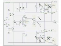
3. If it should be used, what values/devices should be chosen for R17-R22 and the two transistors, all of which are crossed out in the attached schematic?
Fan
I am thinking of mounting a large, slow and quiet fan on the underside of the perforated top that would pull air up and out from below. I have used fans mounted in the back before with good results. I also know of descriptions of external fans to run air by heat sinks. But I was thinking of adding a fan to the underside of the top as an easy addition that would provide a bit more of a safety factor. Any thoughts on this, and which fan might you suggest?
Everyone, you can't imagine how much I appreciate the comments. That's what makes this site so incredibly helpful and educational.
Steve
I am considering a couple safety options I wondered if anyone would comment on.
Current limiting
I built this without the current limiting circuit. The reason was not that I was attempting to make the amp sound better, though I have read of those who firmly believe so, and they may be correct. Rather, I was anticipating that current limiting, as originally designed, would begin limiting before I desired it to do so. In pre-build discussions with a couple of friends, it seemed that it would not be worth it, but I would love to get the thoughts of several persons.
1. Should a current limiting circuit be used (the boards were designed for this option)?
2. If it should be used, at what current would you want to begin limiting in this amplifier given results I've posted on distortion, capping, etc., when considering transient peaks that occur during music (classical or otherwise)?
3. If it should be used, what values/devices should be chosen for R17-R22 and the two transistors, all of which are crossed out in the attached schematic?
Fan
I am thinking of mounting a large, slow and quiet fan on the underside of the perforated top that would pull air up and out from below. I have used fans mounted in the back before with good results. I also know of descriptions of external fans to run air by heat sinks. But I was thinking of adding a fan to the underside of the top as an easy addition that would provide a bit more of a safety factor. Any thoughts on this, and which fan might you suggest?
Everyone, you can't imagine how much I appreciate the comments. That's what makes this site so incredibly helpful and educational.
Steve
Attachments
Steve,
First let me congratulate you on making such fantastic documentation - this thread needs to be stickyed, for sure.") D
D
As for your questions about current limiting and a fan,
Current limiting: Was removed in the F5T. 'Nuff said.
Fan: Have you seen Zen Mod's "babysitters"? http://www.diyaudio.com/forums/pass-labs/186554-babysitter-papas-koan.html#post2530010 A great solotion to the heat issue, IMO
First let me congratulate you on making such fantastic documentation - this thread needs to be stickyed, for sure.
DAs for your questions about current limiting and a fan,
Current limiting: Was removed in the F5T. 'Nuff said.
Fan: Have you seen Zen Mod's "babysitters"? http://www.diyaudio.com/forums/pass-labs/186554-babysitter-papas-koan.html#post2530010 A great solotion to the heat issue, IMO
well - it doesn't matter what I'm thinking ........
just look at fixing points in original FW amps
Zen Mod, I have searched around and attempted to find images that presented enough detail so I could see how circuit boards were secured in the original First Watt amps, but have failed to find what I needed to see. Might you tell me what those fixing points looked like? All four corners (or more)? Or just sides opposite to the output devices attached to heat sinks?
Thanks.
Thanks Zen Mod, Andrew, Bear and flg. Screws and supports now are only in place on the side of the circuit board opposite to the side with MOSFETs.
Steve
point with looking at original FW pcbs is to observe exact (and non critical) points where pcbs are fixed to heatsink
so - distance between pcb fixing points and mosfet pads is .......... same as distance between mosfet screw and mosfet pins
in other words - do not bang your head about that

I am going to build a base with a fan like Zen Mod demonstrated for this amplifier (see post #71). I then will rebias and take temp readings and post my findings. This should only take a couple days, if I can work it in. Thanks, everyone.
bias it to 55C at heatsinks in summer conditions , fanless
then power fan on , it can be powered with small 12VDC wall thingie , equipped with some sort of voltage reg (lm317 good enough)
hopefully amp will stay then in 50C bracket , which is good enough
point with looking at original FW pcbs is to observe exact (and non critical) points where pcbs are fixed to heatsink
so - distance between pcb fixing points and mosfet pads is .......... same as distance between mosfet screw and mosfet pins
in other words - do not bang your head about that
Thanks. In the photos to which you linked, I took the mounting hardward holding the boards to the sink to be on the MOSFETs and at no other location. Obviously I did not interpret things accurately.
I have begun construction of one of Zen Mod's babysitters for providing ventilation. 6L6 linked to Zen's project in post #71.
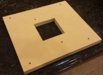
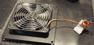
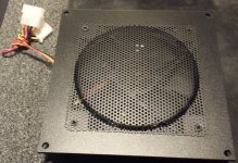
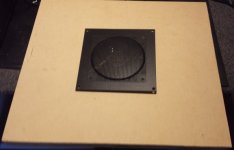
I went through some boxes of spare parts and found a 12 V cabinet/CPU fan with an adapter and a nice cover (can't even remember when I bought it). It was 120 mm X 120 mm and about 1 inch thick.
I glued and screwed together a couple pieces of 1/2 inch high density fiber board to make a stand that was 14 X 16 X 1 inch.
I cut out an opening in the center for the fan.
Next, I'll paint the stand black, add some 7/8th inch feet, and mount a small enclosure on the side for connections and, perhaps, to place a simple power switch on the 12VDC side. These are just some photos of what I've done thus far.
If too noisy, I may cut the voltage to the fan to slow it a bit, but I don't think this will be an issue.
Attachments
- Status
- This old topic is closed. If you want to reopen this topic, contact a moderator using the "Report Post" button.
- Home
- Amplifiers
- Pass Labs
- F5c (cascode) cviller boards 40 V rails build