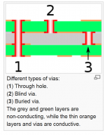
Wikipedia tells you the different types of vias, see attachment & link.
I personally don't put vias directly under IC pads because I worry this will wreck the planarity of the soldering surface, and prevent some of the package legs from touching their PCB solder pads. Giving rise to invisible open-circuits, one of the more difficult PCB troubles to diagnose.
In your drawing I'd probably move the green via to the left by 3 circle-diameters, away from the landing strip where the package leg touches down.
edit- Does this mean I would/should be willing to put vias inside pads of 2-terminal components like capacitors and diodes (which don't require planarity)? Um, err, yes I suppose so.
Attachments
Last edited:
Thanks. That's good advice.
It was the Wiki article that led me to believe these weren't buried/blind.
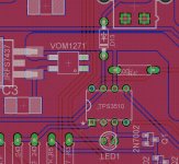
I presume that underneath an IC (not the IC pads) is likely less of an issue? Things are getting rather cramped at one area of this board. I'd like to move the vias to the left here rather than to the right...
It was the Wiki article that led me to believe these weren't buried/blind.
I presume that underneath an IC (not the IC pads) is likely less of an issue? Things are getting rather cramped at one area of this board. I'd like to move the vias to the left here rather than to the right...
Attachments
to the left by 3 circle-diameters
I need to read more carefully the first time...
I exchanged messages with Helmut Sennewald regarding the tweak which stabilises the dual regulator circuit. R6 and C4 reduce the gain of the extra amplifier, i.e. the TL431/SPX431, for high frequencies (I see these two form a low pass filter). However "this pure RC has too much phase shift." "Reduce the loopgain for high frequencies and use the other resistor [R5] to improve the phase margin." I've not yet pursued just how R5 improves phase margin.
Two layouts are presented below, each with its corresponding schematic diagram. Resistors "R sub w" are wiring resistances, namely, the resistances of PCB tracks.
Personally, I find that only one of these two schematic diagrams appeals to my aesthetic sense of what-looks-good. But hey that's just me.
The right hand drawing breaks the rules
Run the input to the capacitor.
Run the output from the capacitor.
Use the left hand drawing. it performs better, particularly at the harmonics of the supply frequency and at the lower frequency interference.
Perhaps you may find that the two schematic topologies produce nonidentical simulation results when room temperature, 1oz/ft2, copper metallized, PCB trace resistances are included. Perhaps the one that looks better, simulates better too. Or perhaps it (surprisingly) does not.
Substitute "impedance" for the resistances labeled Rwt and Rwx
Change the impedance by increasing the inductance and see what effect this has on the signal coming out of the PSU.
Okay, I (finally) did the simulations. Layout on the left has better noise rejection and lower output impedance, particularly at higher frequencies. (The difference is less pronounced, but remains, at lower frequencies i.e. below 100Hz.)
It would seem to me that the layout of the DIYAudio psu board - at least judging by photos of the board - is flawed in this regard.
Simulation lets you quantify the performance difference between two layouts. Then you can ask the question "is this amount of difference significant, or is it insignificant, to me?" One might be "better" than the other, by a very small amount. Or by a whopping, embarrassingly huge margin.
Last edited:
It seems like the gain is free and there to be had. Why compromise?
But I agree that having a sense of perspective requires experience. I have trouble, as this thread has demonstrated at times, judging whether something is worth fussing over. I haven't yet developed a sense of relativity. For example, I have no sense as to whether is the noise rejection I am modelling is fair, good or great. I wonder what the best regulators achieve - if only to have a better sense of what is possible.
I've made some progress with the TPS3510 "control board". See attached image.
I have made the following calculations to determine appropriate values for C1, C2 and C3 for voltage slew rate control ahead of the pass transistors. (The parts in the schematic are placeholders for now.)
Cgate = Cload x Ipu/Imax
where
Cgate = the size of capacitance from gate to ground
Ipu = the current fed to the gate and Cgate
Imax = the maximum permissible current through the pass transistor (in my case, 5A
The circuit I posted in #147 (with the voltage divider of R1 and R2 corrected) should lead to a forward current across the VOM1271 diode of around 30mA. According to the VOM1271 data sheet, a typical open circuit current for an If of 30mA is 47uA. So Ipu = 47uA give or take***.
Earlier I posted the ATX PSU spec for capacitive load:
Using these and the above formula with Ipu of 47uA I get:
Cgate12V = 8,000uF x 47uA/5A = 75nF
(all 12V comes from a single rail in my case)
For the 5V and 3.3V I get 56nF. (The 5VSB voltage supply doesn't go through a pass transistor.)
What I am unsure of is whether being conservative in these calculations or in the selection of the gate capacitors will restrict, adversely, the flow of current once everything is charged.
I can use a ECHU1C563GX9 for the 5V and 3.3V. For the 12V, I have (from the same series of capacitors) 68nF or 82nF available. Dropping 82nF into the above formula and solving for Imax yields 4.6A. If this "throttle" remains fixed post initial charging of Cload then I have restricted the current capability of the power rail.
Perhaps I am better off using 68nF for a maximum current through the pass transistor of 5.5A. Judging from a look at the safe operating area for the IRFS7437PbF, 5.5A burst would appear ok:
*** I am confused when I look at the data sheet for the VOM1271 and compare Electrical Characteristics, Fig 2 and Fig 8. From Electrical Characteristics, If = 30mA => Voc of 8.9V and Isc of 47uA.The former matches Fig 2. The latter, however, seems to clash with Fig 8 when I look at 8.9V on the x-axis...
But I agree that having a sense of perspective requires experience. I have trouble, as this thread has demonstrated at times, judging whether something is worth fussing over. I haven't yet developed a sense of relativity. For example, I have no sense as to whether is the noise rejection I am modelling is fair, good or great. I wonder what the best regulators achieve - if only to have a better sense of what is possible.
I've made some progress with the TPS3510 "control board". See attached image.
I have made the following calculations to determine appropriate values for C1, C2 and C3 for voltage slew rate control ahead of the pass transistors. (The parts in the schematic are placeholders for now.)
Cgate = Cload x Ipu/Imax
where
Cgate = the size of capacitance from gate to ground
Ipu = the current fed to the gate and Cgate
Imax = the maximum permissible current through the pass transistor (in my case, 5A
The circuit I posted in #147 (with the voltage divider of R1 and R2 corrected) should lead to a forward current across the VOM1271 diode of around 30mA. According to the VOM1271 data sheet, a typical open circuit current for an If of 30mA is 47uA. So Ipu = 47uA give or take***.
An externally hosted image should be here but it was not working when we last tested it.
Earlier I posted the ATX PSU spec for capacitive load:
An externally hosted image should be here but it was not working when we last tested it.
Using these and the above formula with Ipu of 47uA I get:
Cgate12V = 8,000uF x 47uA/5A = 75nF
(all 12V comes from a single rail in my case)
For the 5V and 3.3V I get 56nF. (The 5VSB voltage supply doesn't go through a pass transistor.)
What I am unsure of is whether being conservative in these calculations or in the selection of the gate capacitors will restrict, adversely, the flow of current once everything is charged.
I can use a ECHU1C563GX9 for the 5V and 3.3V. For the 12V, I have (from the same series of capacitors) 68nF or 82nF available. Dropping 82nF into the above formula and solving for Imax yields 4.6A. If this "throttle" remains fixed post initial charging of Cload then I have restricted the current capability of the power rail.
Perhaps I am better off using 68nF for a maximum current through the pass transistor of 5.5A. Judging from a look at the safe operating area for the IRFS7437PbF, 5.5A burst would appear ok:
An externally hosted image should be here but it was not working when we last tested it.
*** I am confused when I look at the data sheet for the VOM1271 and compare Electrical Characteristics, Fig 2 and Fig 8. From Electrical Characteristics, If = 30mA => Voc of 8.9V and Isc of 47uA.The former matches Fig 2. The latter, however, seems to clash with Fig 8 when I look at 8.9V on the x-axis...
Attachments
Last edited:
I can't find the posting where you wrote out your full and complete list of design requirements, but (from not-so-reliable-memory) I think I remember that one of them was, approximately,
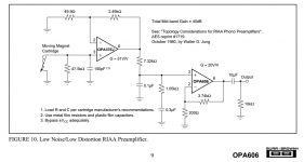
Walt Jung's blog includes a preprint of his AES paper on passively equalized, ultra low noise RIAA amplifiers. Walt's first stage is a pure, flat frequency response, gain-of-25X amplifier block, for optimum signal-to-noise ratio. His later shifted to a gain of 50X in the first stage; if we take the geometric mean, sqrt(25*50) = 35X might be an uncontroversial, fence-straddling choice of first stage gain. But your PCB has no supply-noise-amplifier at all! It is rather a surprise.
Achieve far, FAR lower voltage noise on the final supply rail, than the noise from an Anker E4 Astro battery pack. If this goal is achieved, it annihilates any possible assertions or claims that mains-powered regulated supplies must be inferior, always are inferior in the noise department.
Assuming I remembered correctly, it's rather a big surprise that your PCB layout does not include at least one stage of supply noise sensing, amplification, and buffering, to let you accurately measure noise on your kick-those-guys-in-the-rear-end power supply. I would have thought you'd include a very low noise opamp in a gain-of-35X circuit (AC coupled with a low frequency rolloff well below 20Hz), so you can accurately measure your supply noise without being contaminated by noise from your scope and/or other instrumentation.Walt Jung's blog includes a preprint of his AES paper on passively equalized, ultra low noise RIAA amplifiers. Walt's first stage is a pure, flat frequency response, gain-of-25X amplifier block, for optimum signal-to-noise ratio. His later shifted to a gain of 50X in the first stage; if we take the geometric mean, sqrt(25*50) = 35X might be an uncontroversial, fence-straddling choice of first stage gain. But your PCB has no supply-noise-amplifier at all! It is rather a surprise.
I inadvertently linked to a tiff file above which this website has trouble displaying. (The time limit on post editing is very annoying.) Here's a jpg version:
Looking at this chart again, I probably don't need to worry about any voltage slew rate control for the 3.3V and 5V rails as the LT1084 will limit current within the safe operating area of the IRFS7437PbF pass transistor. An initial 12V Vds on the 12V rail is a little closer to the limit.
I think I can also answer my own question above. The gate capacitor limits the rate of increase of Vgs. Once everything is charged Vgs will be at 8.9V, the transistor fully on and no "throttle" to current flow (except the current limiting of the LT1084).
Mark, I had been wondering about this but from a more general point of view i.e. I was thinking I would eventually have to build some sort of amplifier to put my scope to any decent use. It's an interesting idea to place one on the board itself (presumably with some sort of switching to select which voltage is being measured). With an 'off-board' "scope amplifier" setup I would still need probe points on this board - I was initially thinking I could connect the scope probes to the input connectors but of course connection to the output traces would be preferred.
I will read Walt's paper but what would be the advantages of the measurement amplifier being on this board versus a general-use amplifier that can be used to measure other things as well?
Thanks again
Steve
(I assume from your post you are only talking about taking measurements and not sensing the input voltage and adding another layer of regulation before the output.)
An externally hosted image should be here but it was not working when we last tested it.
Looking at this chart again, I probably don't need to worry about any voltage slew rate control for the 3.3V and 5V rails as the LT1084 will limit current within the safe operating area of the IRFS7437PbF pass transistor. An initial 12V Vds on the 12V rail is a little closer to the limit.
I think I can also answer my own question above. The gate capacitor limits the rate of increase of Vgs. Once everything is charged Vgs will be at 8.9V, the transistor fully on and no "throttle" to current flow (except the current limiting of the LT1084).
Mark, I had been wondering about this but from a more general point of view i.e. I was thinking I would eventually have to build some sort of amplifier to put my scope to any decent use. It's an interesting idea to place one on the board itself (presumably with some sort of switching to select which voltage is being measured). With an 'off-board' "scope amplifier" setup I would still need probe points on this board - I was initially thinking I could connect the scope probes to the input connectors but of course connection to the output traces would be preferred.
I will read Walt's paper but what would be the advantages of the measurement amplifier being on this board versus a general-use amplifier that can be used to measure other things as well?
Thanks again
Steve
(I assume from your post you are only talking about taking measurements and not sensing the input voltage and adding another layer of regulation before the output.)
I took a look at the Walt Jung article. I'm unfamiliar with opamps generally but this is a logical next step for me (and obviously IC regulators themselves are a form of amplifier) and I might guess that this is, in part at least, the reason for suggesting this next 'assignment'. ")
When I look at Fig 2 in the AES article, I see (in sequence) a gain block of 24.7x, (I don't understand the reason for Rt and Ct except that I read they provide "input termination" and "are optimised for flattest response") a transfer function N which boosts low frequencies and reduces high frequencies as required by RIAA equalisation, a further 40.2x gain block and a high pass filter with corner frequency of 1.6Hz. (Perhaps C1 was meant to be 1uF?) One would think that the transfer function N could be removed because we want to observe the actual amplified input (and not certain frequencies attenuated or boosted) but maybe that thinking is a bear trap; else if only one gain block were to be used 35x could be achieved by simply changing R2 to 34k.
As mentioned above, I have for some time had in the back of my mind the need to build an amplifier to accurately measure noise on these (and other) power rails. I noted the work done by Lasse in the "LM317+TL431, really?" thread. His preamplifier would appear to have been rather more complex...
I recommend you figure out what tests you're going to perform on the finished hardware, and also figure out how you're going to perform them. Some of those tests might benefit from modifying the hardware design, specifically to aid testing. In the case of noise testing, perhaps building the first stage of sensing-and-amplifying right into the D.U.T. itself, could simplify later testing. Or perhaps not.
Walt Jung's AES preprint discusses partitioning a high-gain amplifier into two or more pieces. He notes that for best noise performance, the very first stage should have extremely low noise and operate at high gain. That way, the noise of subsequent amplifying stages will be negligibly small -- it's effectively attenuated by the gain of the first stage. There is another benefit: RMS addition of uncorrelated noise sources diminishes the second stage's contribution even further.
However in an RIAA phono preamp, you can't make the first stage gain enormous, else large input excursions like ticks and pops will overload (clip) the amplifier. Jung chooses a gain of approx 25X as a nice tradeoff. Later, (when helping to create) the datasheet for the OPA606, he boosted his recommended gain to 51X, figure below. This offers three possibilities for mindless copycatting: (i) 25X gain; (ii) 51X gain; or (iii) something-in-between-how-about-35X gain.
You might decide that it is preferable to test both power supplies (Anker E4 Astro battery pack, and new mains-powered supply PCB) the exact same way using the exact same noise measuring apparatus for both. When the exact same test gear, used the exact same way, gives better results for Red than for Blue ... Red is the obvious winner. Since it would be very difficult to integrate a low-noise, gain-of-51X preamp into the battery pack, perhaps the conclusion is to measure both supplies using all-external test equipment, and thus omit the preamp from the mains-powered supply PCB. Or you might go ahead and put a supply-noise preamp on the PCB, just to have that measurement option available later. Don't forget to provide a mechanism (jumper?) that shorts the preamp input, so you can measure the noise floor.
edit- Oh by the way, Walt's choice of an OP-37 decompensated opamp for the first stage, is brilliant. Since he's operating it at a closed loop gain of 51X, there is no risk of instability, and he gets all the extra bandwidth that comes with decompensation, for free. The OP-37 is quite a low-noise little devil, to boot. Well done!
_
Attachments
Last edited:
At least if I add this to the board I won't have to wait until I finish another project to measure these supply rails. I will add it.
Understood re 2-stage. I had previously misunderstood your earlier comment in relation to 35x and noted later that it applied only to the first stage. (I also note my typo in my previous post re resistor value.)
So I need to implement:
1. Some sort of switch to select the voltage under test. I assume a 4 position DIP switch would work fine with the 4th position shorting the input to common.
2. Two op-amps in series, the first at 25x-51x gain and the second at circa 20-40x (latter lower if former higher).
3. Decoupling of Vcc for the op-amps.
4. DC decoupling at output.
5. No filter required.
Selecting the op-amps. I did a search at Mouser for OPA37, single channel, SOIC-8 package, single channel. It would appear the Burr-Brown ultra-low noise OPA37 series (from TI) require +/- voltages which would be much less convenient than single +V. Or am I mistaken? Perhaps the OPA376 is a better choice (although I note they don't appear to be de-compensated).
Why is 51x Acl magical - merely because it is greater than the required 5x?
It would appear the Burr-Brown ultra-low noise OPA37 series (from TI) require +/- voltages which would be much less convenient than single +V. Or am I mistaken?
I see they have a quiescent current of max 5.7mA. I wonder if I could use a simple charge pump voltage inverter to provide the -Vcc if required.
If I were you I would start by designing the test apparatus that measures the noise of the Anker E4 Astro battery pack, since that is the hardest problem.
I would assume this apparatus drives an oscilloscope whose sensitivity is set to 2 millivolts per vertical division (or higher, if the noise is really big). Thus your test apparatus needs to have enough gain to amplify the supply noise on the battery V+ output node, from (its actual amplitude) up to at least 3 or 5 millivolts (of output).
Once you've got this apparatus designed, you can decide how much of it to duplicate on your power supply PCBs. Maybe you will decide to duplicate only the first stage (35X??) on your supply PCB? The first and second stages? The entire, complete amplifier? Your decision.
Here is a little food for thought, covering battery noise: (link) I have no idea whether the author is an insane crackpot, a blinding genius, or both, or neither.
SPICE simulations can help you decide whether you've made good, or lousy, choices for AC coupling capacitor placements and values.
Linear Technology's website can help you select a +5V only, single supply opamp with decent noise performance. The LT1677 might be a candidate.
Hi
It is not a priority of mine to measure the noise on a battery setup. The Anker topic came up when I had mentioned, in the context of the LM317+TL431 regulator thread, that I would use that regulator setup to power an SSD. The counter claim was that an SSD already had very good noise rejection (by necessity) and didn't internally run off 5V and so why bother. I merely mentioned that there was a pool of people over at Computer Audiophile who claimed to hear "massive improvement" when powering their SSD from an Anker battery pack. I'm very sceptical, particularly given the data is already in memory prior to playback, but then I had always powered my data SSD with a separate regulator module (a modified simple, LM317-based Velleman module).
I did produce a couple of versions of the LM317/SPX431 DC regulator board (a good learning exercise) and have replaced the Velleman module. I did not pause to compare them. I sent a couple of the spare boards to a friend who used them to power an SSD and a USB card (rather than powering them from the motherboard). He claims they improved the sound a lot. Imagination or real? I don't know.
Perhaps the advantage stems from merely isolating the supply from the motherboard noise. I don't know. Computer audio enthusiasts widely use a SoTM sata filter for their SSDs and claim improvement. I believe this module leaves the data paths untouched but filters the power supply into the SSD/SATA device. It is also claimed that the module blocks SSD/SATA noise from entering the broader PSU. You may recall me asking how noise in a powered module could couple back through to the input side of a regulator module (and I implemented your suggestion of two protection diodes in series with a small cap to ground between them).
What I would very much like to be able to do is measure the results of all this PSU work and see how it performs versus simulations. It may even provide a check against error. As previously noted, if I can readily implement a good amplifier on the board (without too much cost in board real estate or mental contortion) then I will gladly implement it rather than waiting for a measurement amplifier project to be completed before being able to make measurements.
Thanks for reminding me regarding AC coupling the input. This morning I was reading AN1314. While it discusses video signal amplification and transmission, the the concepts and typologies would still seem relevant. (I note the discussion of charge pumps to gain access to dual supply op-amps.) I had in effect already begun modelling AC coupling and DC decoupling yesterday and had noted the cumulative impact of the two LF poles. At the moment I am puzzled as to why the (generic) op-amps show a roll-off in high-frequency but I presume this is related to "gain bandwidth product".
Re op-amp selection, thanks for the heads-up re the LT1677; I will take a look. It's a bit annoying that Mouser don't seem to stock LT parts.
Cheers
Steve
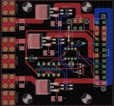
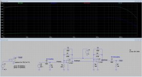
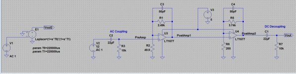
Ok. Proposed circuit addition below. I didn't read anything inthe datasheet regarding sensitivity to decoupling the supply and so didn't bother with this (plus the 5V is already decoupled with a 0.1uF cap at the connection point to the board). The gain is pretty much flat from 15Hz to 55kHz.
60dB of gain. 1000x. My scope has a lowest vertical resolution of 1mV per division. Should be ok. My presumption is that the scope's FFT analysis can show the spectrum of the noise (I've not used this yet).
I also took another look at Lasse's pre-amplifier schematic. It becomes demystified when the switches for gain control are removed. The LT1028 (LT1128 ?) he uses seems to have impressively low noise.
Attachments
Okay, I see a couple of problems...
I pulsed the input voltage and did a transient analysis to look at the results at various stages in the circuit. Obviously there's the issue of clipping if the change in input voltage is too large versus supply voltage/gain. Increasing the supply voltage to 12V provides more headroom. I assume the general problem of potential clipping is unavoidable and places a practical cap on gain for a given supply voltage.
It seems I should add dc decoupling between op-amps. Even when I do this (duplicating the 22uF and 10k resistor) I have a small amount of DC measuring ahead of the first op-amp and second, and a small negative on output.
There's also the poor shape of the waveforms constrained by the slew rate of the op-amp.
I'm sure I am missing something else...
- Status
- This old topic is closed. If you want to reopen this topic, contact a moderator using the "Report Post" button.
- Home
- Amplifiers
- Power Supplies
- Enough current to turn on 3 mosfets?