Mark, I had thought about this but I've previously been warned away here from cascading regulators. I guess I could always sim the typology and see but, frankly, unless I am missing something I already have >150dB ripple rejection. I take on-board your points regarding chassis space and input ripple tolerance but also feel I could go on forever looking at various formulations...I'll give it some thought. 
On the output impedance blip, I scanned Cordell's book for the passages you mentioned but could not find them. (I have not yet read the whole book as I found I didn't have a good enough grounding in transistors to follow much of the amplification sections.) I did find some discussion in 16.4 on resonance peaks and capacitor snubbers.
I didn't get much time on this last weekend as I was feeling the effects of a night out in Munich and a flight back to London which was far too early on Sunday morning!!
One of the reasons why it's probably a good idea to decide upon your important objectives, and your "that's plenty good enough for me" stopping criteria, is that it helps you know when you're done. You don't waste a lot of time needlessly polishing a coprolite. In this case, as soon as you decide how much ripple rejection you want, you can compare that to 150dB and see whether it's okay to move on to other objectives, like stability.
I am away from my books at the moment, but based on the Table Of Contents visible at amazon.com, you might want to have a look at these areas of Cordell's book
I am away from my books at the moment, but based on the Table Of Contents visible at amazon.com, you might want to have a look at these areas of Cordell's book
- 4.6 Probing internal nodes in simulation (p.90)
- 9.3 Frequency response peaking and overshoot (p.180)
- 11.4 Spotting parasitic oscillations (p.227)
- 23.2 Sniffing parasitic oscillations (p.490)
Last edited:
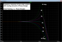
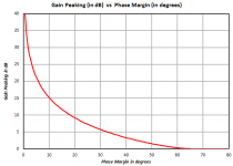
Here's a plot of gain peaking vs phase margin, for a second order negative feedback control system configured as a unity gain amplifier. Your power supply is not a second order system (you've got more than two poles!), nor is it a unity gain amplifier -- your closed loop gain is (5.00volts / Vbandgap) which is about 4.0.
Nevertheless this plot may illustrate in a general way, the reason why designers prefer to see as little peaking as possible, in the closed loop frequency response.
Nevertheless this plot may illustrate in a general way, the reason why designers prefer to see as little peaking as possible, in the closed loop frequency response.
Attachments
Thanks for the pointers re sections of Cordell's book. I will take a look. In the interim, are you saying that the output impedance chart and its peak is related to phase margin and "gain peaking" is related to output impedance? (I fear this is a subject that will really challenge me!)
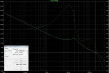
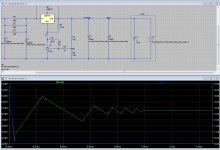
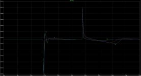
While I peruse Cordell's material over the next couple of days, I attach below a graphic of the stability test output. It indicates a phase margin of circa 49 degrees. I understood an absolute phase less than 180 degrees and a margin in excess of 45 degrees to be stable.
(I also note the trade-off between phase margin and pushing the noise rejection...)
Thanks
Steve
Attachments
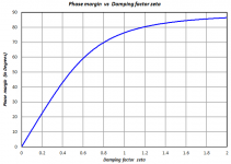
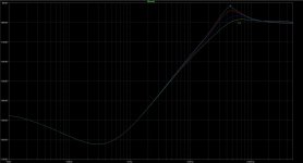
A half hour of Google searching found closed-form equations for phase margin and for gain peaking, of second order linear systems. They are attached below.
I plotted these equations and got a couple of graphs, also attached. If anyone is interested.
I plotted these equations and got a couple of graphs, also attached. If anyone is interested.
Attachments
... are you saying that the output impedance chart and its peak is related to phase margin and "gain peaking" is related to output impedance?
Suppose Edith Engineer attaches a current sink to the output of your (closed loop) voltage regulator. Suppose this current sink sucks 500mA of DC current out of your regulator, plus a sine wave current whose magnitude is 1mA and whose frequency is f Hertz. Thus the current sinusoidally varies between 499mA and 501mA, sucked out of your voltage regulator.
Suppose the Engineer attaches an oscilloscope to the regulator's output and monitors the voltage (probe is AC coupled).
The "input" to this system is the sinusoidal current. The "output" of this system is the very small AC voltage waveform on the oscilloscope.
The Transfer Function (Output/Input) is (Vout/Isink). Volts over Amps equals Ohms. Voila, the transfer function of Edith Engineer's closed loop system, is the output impedance of the regulator. If there is any Gain Peaking in this system, it will appear in the plot of output impedance versus frequency.
On the other hand, in another room, Tim the impatient Technician, connects another current sink to the voltage regulator's output. This current sink pulls a square wave current waveshape out of the regulator. The square wave fluctuates between 12 mA (pulled out of the regulator) and 1.188 A (pulled out of the regulator). Rise time is 200ns, fall time is 200ns, 12mA dwell time is 20us, 1.188A dwell time is 20us, period is 40us. Tim looks at the output voltage and checks to see whether there is any underdamped ringing, or outright oscillation.
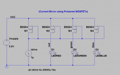
Today I managed to look again at the TPS3510 "switch control". Another view of the timing control diagramme (previously posted) suggests that even when the pass transistor switches are after the regulators (in which case they can be on the TPS3510 board rather than the PSU rails) FPO should still be the trigger. PGO would turn them off too quickly.
I think the attached works, with FPO low placing a current of c30mA across the VOM1271 (PC817A in the circuit) and impressing 8.9V Vgs on the pass transistors (which would be IRFS7437). The two 2N7002 perform the logic control.
I added input caps but I'm not sure these are necessary (although I think they will approximately halve the output impedance bump of the power rails). I've still to work out the correct values for caps C3, C6 and C9 which control slew rate of the pass transistors. (V1 would just come from the 5V pre the pass transistor.)
Paul, you had earlier suggested a cap after the pass transistors (suggesting it be small). I don't understand why one would be necessary.
One rather embarrassing question regarding calculating the value of resistor R3. I was going to use a simple through-hole Kingbright LED for D1. It has a typical forward voltage of 2.2V. For 20mA of current across the resistor (the max that FPO can sink) is the calculation simply (5-2.2)/.02 = 140R. Vf for this thing seems vastly different from any native model in LTspice.
Attachments
Suppose Edith Engineer attaches a current sink to the output of your (closed loop) voltage regulator. Suppose this current sink sucks 500mA of DC current out of your regulator, plus a sine wave current whose magnitude is 1mA and whose frequency is f Hertz. Thus the current sinusoidally varies between 499mA and 501mA, sucked out of your voltage regulator.
Suppose the Engineer attaches an oscilloscope to the regulator's output and monitors the voltage (probe is AC coupled).
The "input" to this system is the sinusoidal current. The "output" of this system is the very small AC voltage waveform on the oscilloscope.
The Transfer Function (Output/Input) is (Vout/Isink). Volts over Amps equals Ohms. Voila, the transfer function of Edith Engineer's closed loop system, is the output impedance of the regulator. If there is any Gain Peaking in this system, it will appear in the plot of output impedance versus frequency.
On the other hand, in another room, Tim the impatient Technician, connects another current sink to the voltage regulator's output. This current sink pulls a square wave current waveshape out of the regulator. The square wave fluctuates between 12 mA (pulled out of the regulator) and 1.188 A (pulled out of the regulator). Rise time is 200ns, fall time is 200ns, 12mA dwell time is 20us, 1.188A dwell time is 20us, period is 40us. Tim looks at the output voltage and checks to see whether there is any underdamped ringing, or outright oscillation.
Very helpful. I will read why Edith worries about this and also perform Tim's test!
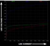
I ran a DC sweep simulation using the three LED .MODELs on the CordellAudio.com website. They are provided by Bob Cordell himself. An LED with Vfwd = 2.2 volts, would fall between the green curve and the blue curve. Pretty close to the green curve.
Attachments
You can connect an ideal current source to the output, that switches from 95% of Iload_max, to 5% of Iload_max, in less than 200 nanoseconds. If this step function current produces non-damped oscillations near the impedance bump frequency (250 kHz), that would be a concern. IIRC Bob Cordell's book discusses closed loop gain-peaking {on log axes} and suggests worry-thresholds for how tall a peak can be before it becomes worrisome.
In SPICE you'd use a PULSE current source, with risetime=200ns, falltime=200ns, high time=20us, low time=20us, period=40us. This lets you observe the 5%-to-95% transition, and the 95%-to-5% transition. Your circuit will handle one of them far worse than it handles the other. But which? Why predict, just simulate both and let SPICE tell you.
Suppose Edith Engineer attaches a current sink to the output of your (closed loop) voltage regulator. Suppose this current sink sucks 500mA of DC current out of your regulator, plus a sine wave current whose magnitude is 1mA and whose frequency is f Hertz. Thus the current sinusoidally varies between 499mA and 501mA, sucked out of your voltage regulator.
Suppose the Engineer attaches an oscilloscope to the regulator's output and monitors the voltage (probe is AC coupled).
The "input" to this system is the sinusoidal current. The "output" of this system is the very small AC voltage waveform on the oscilloscope.
The Transfer Function (Output/Input) is (Vout/Isink). Volts over Amps equals Ohms. Voila, the transfer function of Edith Engineer's closed loop system, is the output impedance of the regulator. If there is any Gain Peaking in this system, it will appear in the plot of output impedance versus frequency.
On the other hand, in another room, Tim the impatient Technician, connects another current sink to the voltage regulator's output. This current sink pulls a square wave current waveshape out of the regulator. The square wave fluctuates between 12 mA (pulled out of the regulator) and 1.188 A (pulled out of the regulator). Rise time is 200ns, fall time is 200ns, 12mA dwell time is 20us, 1.188A dwell time is 20us, period is 40us. Tim looks at the output voltage and checks to see whether there is any underdamped ringing, or outright oscillation.
Ok this has been extremely helpful already. I had looked at transient and loop stability on a previous version (different values for R4 and R5) and thought things stable. However, I did this with a 0.1A load. I couldn't understand why the circuit oscillated when I added the rectification and filter caps to look at currents through them with 5A load. The load affected stability. I'm now questioning everything I've looked at regarding stability. The loop stability test with this current circuit, a 0.1A active load and 50mA resistive load (I should just delete this I guess) showed phase margin of 49 degrees and gain margin of 18.7dB. When I increased the active load to 5A I had phase margin of just 4 degrees and gain margin of 4.4dB.
I'm reading the Cordell material. Phase does my head in but I'm determined to get there.
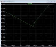
In the interim, here's a stepping of load from 0.25A for 20us to 4.75A for 20us (5% Iload_max to 95% of Iload_max) and back again. Doesn't seem great and I presume this a better way to load a transient test than my previous work of a 0.1A step (?) which obviously looks a lot better. I'm not sure how to look at this in the frequency domain except to measure the length of each half wave, observe the frequency shown in the bottom left corner of the screen and divide these by two. None seem to coincide with the frequency at which output impedance blips up.
Obviously the circuit doesn't handle a step up in load well at all. In fact, if I do a simple step from zero to full load the voltage never recovers. I'm struggling as to why. If the reg can handle 5A surely the voltage should recover...
Attachments
Yes that waveform does indeed look terrible. If I were you, I wouldn't send the PCBoards to fab just yet.
Remember that the LT voltage regulator integrated circuit has real transistors inside. One of them is the output transistor. Its transconductance is proportional to its collector current (hybrid pi model): gm = Icollector / (kT/q). So when you increase the output current from 100mA to 5000mA, the transconductance increases by 50X.
Depending on internal IC design details, this might easily scoot the Output Pole to the right (higher frequency) by factor of 50X, and move it uncomfortably close to the ESR Zero. This would reduce phase at the unity gain crossover, and thus, reduce phase margin. TI has some nice articles about the ESR Zero and how it compensates for the Output Pole
If these effects are indeed included in the Linear Technology SPICE macromodel for their voltage regulator, you can observe them in simulation. Open loop frequency response at low, middle, and high values of output current would indicate whether output stage gm effects, are or are not being modeled.
edit- the 2nd trough, at t=0.53 milliseconds, might include some high speed sinusoidal oscillations too. The wiggles look suspicious. You may want to zoom in there and take a look.
Last edited:

Oh let's just ignore all the above...there's a glaring error in the transient circuit that somehow evaded my attention. Time for a break. I will pick this up again tomorrow.
This is with the right IC. Still needs fixing however...
This is with the right IC. Still needs fixing however...
Attachments
Last edited:
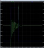
Zounds! Now that right there is an underdamped control system.
We can use the method of logarithmic decrement to extract the damping factor zeta. (Wikipedia covers logarithmic decrement) and so does the Quasimodo design note's Appendix B.
On my zoomed-in printout of the waveform in post #154, the 2nd waveform trough is 95 millimeters tall, and the 10th waveform trough is 16 millimeters tall. Thus the logarithmic decrement has N=8, V1=95, V2=16; giving delta = 0.223 and zeta = 0.035.
Cowabunga! The system appears to be wildly underdamped (zeta = 0.035). Extracting phase margin from the damping factor, using the closed-form equation in post #145, the phase margin is four degrees. Not forty degrees, four degrees. Borderline unstable, I'd say.
Last edited:
I had looked at transient and loop stability on a previous version (different values for R4 and R5) and thought things stable. However, I did this with a 0.1A load. I couldn't understand why the circuit oscillated when I added the rectification and filter caps to look at currents through them with 5A load. The load affected stability. .... The loop stability test with this current circuit, a 0.1A active load and 50mA resistive load (I should just delete this I guess) showed phase margin of 49 degrees and gain margin of 18.7dB. When I increased the active load to 5A I had phase margin of just 4 degrees and gain margin of 4.4dB.
Well at least everything triangulates! I will study your last post to ensure I follow it all and also look at stability under full load. Thanks again.
Ok. So I did a bit of reading on second order linear systems. I haven't been confronted by that sort of mathematics since high school! For now I will have to take a lot of it on faith but at least I now recognise that a system response with ringing/oscillation is at least of second order. (I still struggle with concept of poles and zeroes.) I will read more.
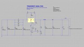
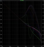
I did some further work on the circuit (see attachments). My approach was as follows. Set R4 to ensure that the cathode of the SPX431 or TL431 had minimum current for regulation. This is a typical 0.4mA and max 1.0mA. I set R4 to ensure Ik of just over 1mA.
I profess to not understanding the RCR filter of R5, C4 and R6 properly and would greatly appreciate a better understanding of it and it's impact on the feedback loop. Rightly or wrongly I view it as a "bypass" around the TL431. On this basis, I looked at varying just R5 expecting to see a lower R5 improve stability and transient response and worsen noise rejection.
The second attachment shows the impact on transient response of varying R5 (stepping from 0.25A to 4.75A and back again; lesser load steps produce less ringing): 11K, 8.5K, 6K, 5K. It is interesting to note the trade-off between a step up in load and a step down. My presumption is that one seeks a result that balances both to the best degree possible. Perhaps somewhere between 8.5k and 6K.
The third attachment shows the impact on noise rejection. Not as bad as I had thought it might be. As load increases (not depicted) the flattening in noise rejection from c60kHz observed in this graphic does not occur and noise rejection continues to weaken.
Loop gain analysis was interesting and seemingly more complex. Phase margin (0dB frequency) results - stepping R5 as above - for a 5A load were:
R5=11K: 51 degrees (415kHz)
R5=8.5K: 42 degrees (66kHz)
R5=6K: 88 degrees (221kHz)
R5= 5K: 92 degrees (176kHz)
Loop gain and phase seem to vary with load in a rather interesting manner. Setting R5 to 6K, I stepped the load from 0.1A to 5A in 0.5A increments. (LTspice rounds off the last odd increment.) The results are shown in the fourth attachment. Note how, as load increases, the 0dB frequency shifts to the right but phase margin initially increases and then falls.
So... a bunch of variable analysis suggesting that the circuit benefits from reducing R5 to between 8.5K and 6K but little understanding as to why this is the case...
Cheers
Steve
(I still struggle with concept of poles and zeroes.) I will read more. I did some further work on the circuit (see attachments). My approach was as follows. Set R4 to ensure that the cathode of the SPX431 or TL431 had minimum current for regulation. This is a typical 0.4mA and max 1.0mA. I set R4 to ensure Ik of just over 1mA.
I profess to not understanding the RCR filter of R5, C4 and R6 properly and would greatly appreciate a better understanding of it and it's impact on the feedback loop. Rightly or wrongly I view it as a "bypass" around the TL431. On this basis, I looked at varying just R5 expecting to see a lower R5 improve stability and transient response and worsen noise rejection.
The second attachment shows the impact on transient response of varying R5 (stepping from 0.25A to 4.75A and back again; lesser load steps produce less ringing): 11K, 8.5K, 6K, 5K. It is interesting to note the trade-off between a step up in load and a step down. My presumption is that one seeks a result that balances both to the best degree possible. Perhaps somewhere between 8.5k and 6K.
The third attachment shows the impact on noise rejection. Not as bad as I had thought it might be. As load increases (not depicted) the flattening in noise rejection from c60kHz observed in this graphic does not occur and noise rejection continues to weaken.
Loop gain analysis was interesting and seemingly more complex. Phase margin (0dB frequency) results - stepping R5 as above - for a 5A load were:
R5=11K: 51 degrees (415kHz)
R5=8.5K: 42 degrees (66kHz)
R5=6K: 88 degrees (221kHz)
R5= 5K: 92 degrees (176kHz)
Loop gain and phase seem to vary with load in a rather interesting manner. Setting R5 to 6K, I stepped the load from 0.1A to 5A in 0.5A increments. (LTspice rounds off the last odd increment.) The results are shown in the fourth attachment. Note how, as load increases, the 0dB frequency shifts to the right but phase margin initially increases and then falls.
So... a bunch of variable analysis suggesting that the circuit benefits from reducing R5 to between 8.5K and 6K but little understanding as to why this is the case...
Cheers
Steve
Attachments
Maybe the place to start is your design notebook. Find the earliest page in your notebook, where you first began to experiment with a cascade of (a 317-style voltage regulator, plus a 431-style shunt regulator taking its input from 1/2 the regulated output & driving the 317's ADJ pin).
Then figure out who suggested that idea: was it an app note, a book, one or more postings on diyAudio, a suggestion from a smooth talking salesman at a high end audio store, a copy-and-paste from someone else's schematic? If printed matter, read it again, read the ancillary materials, track down the bibliographic references, and read some more. If a human being, ask them many questions. Show your simulations and ask, "Is this what I should be seeing?" Why is this component here? Why did you omit this-other component entirely? Since the RCR network between ADJ and cathode (C4, R5, R6) is giving you a temporary flummox-deluxe, ask about that.
Re: 4 degrees phmargin. This is one of those happy times when you get to say with all sincerity, and profound relief: Science Works!
The suggestion came when I was first looking at stability with the LM317-based circuit and had asked a question on the LTspice forums regarding modelling stability tests. Helmut Sennewald edited the circuit. As it's not an LTspice question, I will contact him off-list and hopefully he will respond.
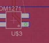
Is placing a via directly underneath a pin of an SMD part "bad form"? I think it's impossible to route my TPS3510 board without using vias... To the novice it would seem more efficient to place the via directly under the pin rather than next to it followed by a short surface trace. I will be using SeeedStudio Fushion PCB. They don't permit "blind" or "buried" vias (nor tented I believe) but I believe these are different.
Attachments
- Status
- This old topic is closed. If you want to reopen this topic, contact a moderator using the "Report Post" button.
- Home
- Amplifiers
- Power Supplies
- Enough current to turn on 3 mosfets?