One way to experimentally "ignore trace resistance" (or more generally, trace impedance) is to use .PARAMs in LTSPICE. The "LIST" option allows you to run three or five or twenty simulations with different values of the params, and plot all simulation results overlaid on the same output graph. You can step the trace resistance/impedance from high to medium to low to near-zero, and see the effects (if any) upon circuit behavior.
PCB copper trace resistance "calculators" abound on the internet; all you do is input the thickness of your copper layer (in oz/ft2), the width of your trace, and the PCB temperature. Then, presto, they spit out the trace resistance per unit length. It might surprise you to see that one inch of PCB trace has a greater resistance than SGK's MOSFET switch -- but it does. Really.
Copper trace impedance "calculators" are also online, but less numerous. They cover microstrip layouts, stripline layouts, and coplanar waveguide layouts {Wikipedia discusses each of these}, and spit out inductance-per-unit-length, capacitance-per-unit-length, characteristic impedance, propagation velocity, and so forth. If you want to simulate impedance instead of resistance, these can help.
I myself would use the methodology outlined in post #115 to decide between the two layout styles. I might even vary the trace resistance above, and below, the real-world number, just to see whether the difference between the two layouts becomes shockingly huge if we make PCBs traces out of high resistance tungsten (or out of zero resistance superconductors). Maybe LayoutX is vastly superior to LayoutY in one of these what-if scenarios, despite X&Y being nearly-indistinguishable in the copper trace scenario. It's likely I would choose X rather than Y for this very reason. But hey that's just me.
Are we talking across purposes? All else being equal, shorter traces are better (lower impedance) - agreed. I questioned whether the circuits illustrated were fundamentally different well beyond just the extra track length that one has. AndrewT seemed to think they were:
No, they are not the same.
The input must go TO the capacitor/s
The output must come FROM the capacitor/s.
The return route should try to follow the flow route.
but I suspect that's what I labelled "flow rather than nodal thinking", the very trap I might have fallen into....
It might surprise you to see that one inch of PCB trace has a greater resistance than SGK's MOSFET switch -- but it does. Really.
Indeed. It was when I was looking at a trace width calculator which also calculated resistance that it sunk home that placing this switch after the regs was perfectly fine...
The two circuit schematic diagrams have different topologies (patterns of interconnected elements) as well as different resistance values. Repeating my urging in post #115, I encourage you to draw the two schematic diagrams yourself, and observe these two different topologies yourself. Perhaps one of the schematics may appeal to you more than the other; I called it aesthetics, you might have a different name for this.
If you decline to rely upon aesthetics, you can simulate the two topologies to see whether one or the other gives more appealing results. If one is even slightly better than the other (one part in ten? one part in 200??), you might as well select that one since both choices have equal cost.
"Tell me the answer?" types of inquiries don't appeal to me very much. What I prefer are "Help me figure out how I can discover the answer myself?" kinds of requests. And I like "Here is my analysis, would you critique it please?" solicitations, best of all. But hey, that's just me.
Last edited:
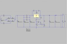
Ok so I did a little test in LTspice to confirm that the attached two circuits produce identical waveforms. (The lower schematic is a more aesthetically pleasing presentation.) LTspice ignores trace resistance and so I conclude that if the trace resistance = 0 waveforms are identical then the board layout with the least trace length (all else being equal) wins. Were I to redo the board in #114 I would take a more direct route to the pass transistor than the trace snaking from C2. The boards are functionally the same (if the pass transistor is off both caps still charge) but the board layout with the longer trace from C2 to the pass transistor involves greater trace length and greater impedance, a cost it needn't incur.
Hopefully that deals with the nagging concern I had...
Hopefully that deals with the nagging concern I had...
Attachments
Here is my analysis, would you critique it please?
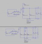
Two layouts are presented below, each with its corresponding schematic diagram. Resistors "R sub w" are wiring resistances, namely, the resistances of PCB tracks.
Personally, I find that only one of these two schematic diagrams appeals to my aesthetic sense of what-looks-good. But hey that's just me.
Attachments
I absolutely agree that the schematic on the left is more aesthetically pleasing and would be how I would (and did) write the schematic (when skipping trace resistances). When I came to draw the board, indeed I followed the 'flow' of the schematic, ignored the air-wire guidance and drew Rw5. My hesitation stemmed from looking at the likes of the Universal PSU board, which has a schematic drawn in the aesthetically pleasing style yet a board which places C2 on a spur like trace-wx in your second graphic.
Now, perhaps I can simplify your second graphic slightly to shift trace-wy to the right such that trace-ws and trace-wt collapse to a trace identical to trace-w3 in your first graphic. Can I not then directly compare the parallel resistances Rwx (=Rw4) and Rwy with the series resistances Rw4 and Rw5 (noting that all else is the same in both cases)? Would I not conclude that the former presents a lower resistance to the circuit? If this is nonsense then I'm all for the aesthetic "flow" approach which is where I started. Presumably I then reject implementations such as the Universal PSU board as being sub optimal...perhaps for the reasons listed by Andrew?
Now, perhaps I can simplify your second graphic slightly to shift trace-wy to the right such that trace-ws and trace-wt collapse to a trace identical to trace-w3 in your first graphic. Can I not then directly compare the parallel resistances Rwx (=Rw4) and Rwy with the series resistances Rw4 and Rw5 (noting that all else is the same in both cases)? Would I not conclude that the former presents a lower resistance to the circuit? If this is nonsense then I'm all for the aesthetic "flow" approach which is where I started. Presumably I then reject implementations such as the Universal PSU board as being sub optimal...perhaps for the reasons listed by Andrew?
Perhaps you may find that the two schematic topologies produce nonidentical simulation results when room temperature, 1oz/ft2, copper metallized, PCB trace resistances are included. Perhaps the one that looks better, simulates better too. Or perhaps it (surprisingly) does not.
If an enthusiastic design student asked me for advice on how to figure it out for himself, I would recommend the exercise in the preceding paragraph.
If an enthusiastic design student asked me for advice on how to figure it out for himself, I would recommend the exercise in the preceding paragraph.
Thanks guys. I intend to do some modelling in this regard, hopefully tomorrow or Sunday.
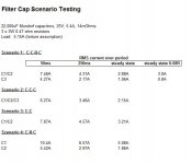
I've been busy modelling filter cap configurations in LTspice and also refining the regulation circuit. 5V only at this stage. Test circuit for filter cap tests and results are appended below.
I attempted to model the start 25C resistance of an NTC CL-80 ICL by, as previously noted, converting the 47R primary resistance into a secondary equivalent. 230V mains transformer, 10V secondary, turns ratio (K) =230/10=23. K^2=529. Rs =Rp/(K^2)=89mR. I note that as the ICL heats with current its resistance will fall. As load current falls its temperature will fall and resistance rise. I did not attempt to model this and simply used a fixed resistance. When reading the datasheet, I'm unsure about the implications of the stated minimum end of the current range and whether this means there has to be a minimum load...
I noted the way that adding an additional cap (from 2 to 3) spread the 'ripple burden' and how adding the resistors shifted the balance between pre- and post- resistor bank capacitors. I also noted how the resistors change the shape of the voltage waveform going into the LT1084. I've heard people say that they prefer a more rounded waveform as this supposedly makes the job of the regulator easier (I assume because the rate of change in the feedback network is less).
It seems to me that it may well be beneficial to add another input capacitor (total of 3) and, if indeed the foregoing sentence is true, to add the resistor bank even if this is a regulated circuit. The resistor bank will also help burn off some of the voltage headroom I have if I stick with a 10V secondary.
Output caps are a lot smaller. I've added a pic of output impedance, transient and noise rejection. Loop gain analysis suggests the circuit should be stable.
Regards
Steve
Attachments
LTSPICE fast fourier transform can quantify the roundedness of the waveform for you.I also noted how the resistors change the shape of the voltage waveform going into the LT1084. I've heard people say that they prefer a more rounded waveform as this supposedly makes the job of the regulator easier
Burn off some of the unnecessary voltage headroom
might be an important insight. You could consider it an advantage, to be exploited. Maybe one or more of
Increased resistor values
Resistor between bridge and first capacitor
Series resistor between the first capacitor's bottom plate, and ground (i.e. in series with ESR). Reduces capacitor ripple current to any value you select.
Smaller capacitors first (nearer the bridge), bigger capacitors last (nearer the output)
Resistor between bridge and first capacitor
Series resistor between the first capacitor's bottom plate, and ground (i.e. in series with ESR). Reduces capacitor ripple current to any value you select.
Smaller capacitors first (nearer the bridge), bigger capacitors last (nearer the output)
Thanks! I will take a look tomorrow.
Right now I am staring at a few parts from my latest Mouser order which was delivered today. (No problems again, Andrew.) I ordered a few parts that I expected I'd use in this project to achieve the free delivery mark. I may need to rethink a couple of them...
I knew the Fairchild 2N7002 in SOT-23-3 was going to be small but it isn't until I looked at one for the first time that I realised I may have bitten off more than I can chew on that one!
I will practice my solder paste and skillet soldering on my LM317/SPX431 DC regulator board which has a ECH-U1C102GX5 and a few ECH-U1H104GX9.... Actually, if I can manage these I may as well use more SMD/SMT parts on the TPS3510 board!
Quasimodo v3 had two SOT23-3s; everyone who bought the kit, assembled it successfully.
Put the tiniest film of solder on one of the 3 pads; a corner pad is better than a middle. Hold the pkg in place with tweezers, melt the leg onto the soldery pad and let it cool. Use that tack-solder job to hold the pkg in place while you solder the other two legs onto their pads. Then resolder the first, original leg onto its pad with a proper amount of solder.
Put the tiniest film of solder on one of the 3 pads; a corner pad is better than a middle. Hold the pkg in place with tweezers, melt the leg onto the soldery pad and let it cool. Use that tack-solder job to hold the pkg in place while you solder the other two legs onto their pads. Then resolder the first, original leg onto its pad with a proper amount of solder.
Thanks for the confidence boost re the SOT-23-3.
Well, I spent the better part of today running simulations rather than working. Quite a complex set of trade-offs tweaking cap values, R from bridge, R values for CCRC filter etc while observing power dissipation across the resistors, 2nd harmonic of voltage waveform into the LT1084 etc etc.
I'm not sure I'm that much more advanced. Adding some resistance directly after the bridge rectifier makes sense as does increasing the resistance in the resistor bank of the CCRC. But it doesn't take much to blow 3W resistors (5A torture load, integral of first second of waveform). 5W resistors are huge (24x8mm).
On smaller caps at the front of the CCRC I found that while ripple dropped, ripple headroom (measured versus max permitted) fell. It also didn't seem to be beneficial to the shape of the waveform into the reg. (Or did you mean smaller filter caps and larger output caps post the reg?) (I did notice that adding another large cap just before the reg boosted noise rejection a bit at 20kHz.)
So perhaps a 28mOhm resistor between bridge and first cap (2.3W dissipation first second, steady state slightly lower) and stepping up the 3 resistors in the CCRC filter to 0.68R (2.4W). With 3 x 22kuF caps, no base resistors, the 200Hz harmonic ripple going into the reg is 7.2mV.
... the 200Hz harmonic ripple going into the reg is 7.2mV ...
What is your stopping criterion, your "good enough for me" finish line? Presumably it's stated in terms of output ripple, which is input ripple divided by 2.2E3 (LM317), or input ripple divided by 3.5E3 (LT1084).
Have you met this design objective yet? Or do you need further iteration?
Attachments
Last edited:
With respect to noise rejection, I would say that if the modelling of this circuit is even close to reality then I am there.
If there's some easy yardage to be had, for example for capacitor longevity, safety or other reasons, then I'll take it but PSRR seems rather good.
I've still got to look at the 3.3V (and 12V) and the power that will need to be dissipated by the LT1084 in that case will be large. Maybe I should provide for another series resistor after the bridge. Everything will be well heat-sinked though.
I have one of these as my IEC entry for EMI/RFI rejection.
I was planning to wire the NTC RCLs between the IEC inlet and the switch.
One thing I was wondering about was output impedance. Model output below. The bump seems tiny to me but one person suggested I try to reduce it.
I still need to look at that trace resistance modelling before working on the boards and of course I need to revisit the TPS3510 "control board". Still lots more to do.
An externally hosted image should be here but it was not working when we last tested it.
If there's some easy yardage to be had, for example for capacitor longevity, safety or other reasons, then I'll take it but PSRR seems rather good.
I've still got to look at the 3.3V (and 12V) and the power that will need to be dissipated by the LT1084 in that case will be large. Maybe I should provide for another series resistor after the bridge. Everything will be well heat-sinked though.
I have one of these as my IEC entry for EMI/RFI rejection.
I was planning to wire the NTC RCLs between the IEC inlet and the switch.
One thing I was wondering about was output impedance. Model output below. The bump seems tiny to me but one person suggested I try to reduce it.
An externally hosted image should be here but it was not working when we last tested it.
I still need to look at that trace resistance modelling before working on the boards and of course I need to revisit the TPS3510 "control board". Still lots more to do.
You can connect an ideal current source to the output, that switches from 95% of Iload_max, to 5% of Iload_max, in less than 200 nanoseconds. If this step function current produces non-damped oscillations near the impedance bump frequency (250 kHz), that would be a concern. IIRC Bob Cordell's book discusses closed loop gain-peaking {on log axes} and suggests worry-thresholds for how tall a peak can be before it becomes worrisome.
In SPICE you'd use a PULSE current source, with risetime=200ns, falltime=200ns, high time=20us, low time=20us, period=40us. This lets you observe the 5%-to-95% transition, and the 95%-to-5% transition. Your circuit will handle one of them far worse than it handles the other. But which? Why predict, just simulate both and let SPICE tell you.
In SPICE you'd use a PULSE current source, with risetime=200ns, falltime=200ns, high time=20us, low time=20us, period=40us. This lets you observe the 5%-to-95% transition, and the 95%-to-5% transition. Your circuit will handle one of them far worse than it handles the other. But which? Why predict, just simulate both and let SPICE tell you.
The resistor bank will also help burn off some of the voltage headroom I have if I stick with a 10V secondary.
Maybe you have so much excess voltage that you could actually take a page from John Curl's preamp playbook: use a cascade of two voltage regulators to attenuate ripple by (60dB_reg1 + 60dB_reg2): >100 dB!! Running the numbers using (mains nominal ACvolts times 90%), and (2x rectifier V_fwd_max), and (thousands of millivolts of ripple going into the first regulator), and (Vdropout specifications from regulators' datasheets), it looks quite feasible. But check it for yourself, I might have flubbed the arithmetic.
Although the semiconductors probably cost more than the 3000-hour-lifetime-at-125C, dozen-millifarad electrolytic capacitors, the semis occupy less PC board area and FAR less chassis volume (esp. height). They also tolerate far more input ripple, thus allowing much smaller diode-charges-capacitor current peaks, thus alleviating your worries in this department.
- Status
- This old topic is closed. If you want to reopen this topic, contact a moderator using the "Report Post" button.
- Home
- Amplifiers
- Power Supplies
- Enough current to turn on 3 mosfets?