Between work, family commitments and the flu I haven't had a lot of time to devote to this over the last week. I decided to try to complete the modelling of the PSU rails before continuing with the layout of the TPS3510 "control" board.
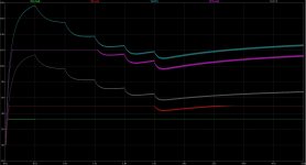
I've encountered a few obstacles which I am grappling with. The first related to stabilising the 3V3 circuit which seems to require lowering the frequency level at which loop gain is reduced by the RCR filter skirting the TL431. I increased the value of the C from 1n to 2.7n. The second obstacle which I have still to address properly is the 12V circuit which, oddly, is stable at low and high currents but appears unstable for a range of load currents in between. (Stepping load from 0.1A to 5A in 1A increments and observing noise rejection shows a complete curve-ball when the load is 2.25A.) I need to spend some more time with this.
The third potential problem appears to be related to the NTC in-rush current limiter. I don't have a Spice model for the particular ICL we were discussing earlier, but I did find one for the EPCOS B57237S330M51 which has a current rating of 2.5A and a resistance at 25C of 33R (versus 3A and 47R for the one we'd previously discussed). I used this and aggregated all 3 power rails into one model for the purposes of examining currents and output voltages for various load conditions. Stepping the rail loads up from 0.01A to 1, 2, 3, 4 then 5A over 0.5s increments flags a potential issue related to the ICL. I conclude that it needs to be bypassed after the initial in-rush else initially it presents too much resistance to an increasing load. I will have to figure out how this can be done, perhaps by re-reading the thread discussing the diyAudio in-rush board. (I wonder if it would not be simpler to deploy such board in my project...)
If interested, a folder with this LTspice model and related components can be found here. I'm not sure if my toroid inductance assumptions make sense. The manufacturer provided me with typical resistance values but not figures for inductance (yet).
PS: Disappointingly this exercise also appears to highlight a problem with the 3V3 and 12V power rails with low loads which will need to be investigated. Ugh, this is wearing me down.
Attachments
Last edited:
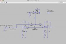
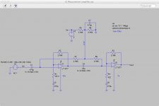
As I was trying to finalise this circuit, I went back over the later posts here - in particular Andrew's comment re input impedance in #190 and Mark's comments in #195 and #197 - and AN-581 once more.
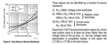
I understand the input impedance of this circuit doesn't need to be so high in order not to affect what it is measuring (as the power rails have very low output impedance). I also understand that the noise of the LT1677 is lowest when the resistance seen by its input pins is lowest (Fig 8 in the data sheet).
If I have read AN-581 correctly I also understand it is desirable to match reasonably the impedance see by each of the op amp input pins.
All this and wanting to set the poles sensibly makes for quite a cocktail for confusion. I found myself going around in circles for awhile.
Am I right to say that the non-inverting input of the circuit as shown sees 4.99k Ohms in series with another 4.99k (2 x 4.99k in parallel), i.e. 10k, and that the inverting input of the first op amp sees 4.99k Ohms in parallel with 127R i.e. something less than 127R? Should I really be scaling resistors R1/R2 (and R3/R4) to better match the non-inverting input impedance and or endeavouring to lower further both input impedances? (To keep the poles/bandwidth C1 (and C2) will need to scale higher as R7/R8 are reduced.)
(I settled on first stage gain of 40x as lower numbers showed gain peaking in high frequencies which I understand risks instability. The loss in bandwidth from a higher gain was not massive. 3dB points are still about 4Hz to 250kHz.)
Attachments

To see the input offset voltage contribution from unequal resistances, you need to confine your analysis to DC. Replace all capacitors by open circuits and replace all inductors by short circuits to perform the DC analysis.
Post_202_U1_Vin+ sees 5K + (5K || 5K) = 7.5K
Post_202_U1_Vin- sees 5K
The offset voltage contribution is {(IB+IOS)*7500} - {IB*5000} = (7500*IOS) + (2500*IB).
Substituting the datasheet worst case max values (IB=600nA, IOS=150nA) we find the offset voltage contribution is (7.5E3*1.5E-7)+(2.5E3*6.0E-7) = 2.63 millivolts DC at the inputs. Multiplying by the stage gain (40X) that's an offset of 0.11V at the output. In my opinion, not much of a problem given that the output can swing 5 volts. The worst case, maximum possible offset can potentially steal 2.2% of your first stage's output swing. No big deal.
Since you followed the first stage with a second amplifier whose gain is 7X, this means you expect the first stage's output is less than (Vsupply / 7) = 0.71 volts. So an offset voltage of 0.11V at the first stage's output, does not put the output anywhere near clipping. No harm done.
Well that was a pretty shocking piece of basic circuit analysis on my part - especially the miscalculation of parallel resistance...
Thanks. That's very helpful.
Am I right then that the revisions below which lower source resistance for the op amps should pull the circuit down the LT1677 noise curve? The impact to the 3dB range is immaterial. Perhaps this is polishing a coprolite as you might say but... (I left C4 at 22u as it doesn't appear to matter.) Either with this version or the last I think I am almost done with this, hopefully.
Oh, there's no discussion in the data sheet about bypassing Vs at the op amp; is it still advisable to do so?
Attachments
No takers on the above? I've allowed room for the larger 470u caps on the board but if I can grab some room back it would be good.
Uber basic question: "short[ing] the pre-amp input" involves simply an open circuit for the input (no connection to a voltage rail that would otherwise be measured) or connecting the input to ground?
Don't forget to provide a mechanism (jumper?) that shorts the preamp input, so you can measure the noise floor.
Uber basic question: "short[ing] the pre-amp input" involves simply an open circuit for the input (no connection to a voltage rail that would otherwise be measured) or connecting the input to ground?
I hope everyone had a great Christmas!
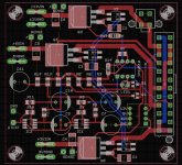
Slow progress being made here. Regarding my last question above, I think the right answer is to tie that input to ground and so this is what I have done. For the measurement pre-amp I have stuck with the circuit in #205. I've not bypassed specifically the power supply to the op amps. Current limiting caps C1, C2 and C3 are still placeholders for now.
Schematic and board layout attached. (I've shown the board without the top and bottom ground planes for better visibility.)
Comments and corrections greatly appreciated. Soldering this will be a lot of fun...
Attachments
SGK,
Remove C1, C2, C3. These only serve to slow the turn on time and don't do anything useful. In fact they will probably cause Q3, Q4, Q5 to overheat during turnon. Remember that the VOM1271 produces an output of 8 volts aprox at 20mA of LED current, but has a source impedance of aprox 300 Kohm, any capacitance on its output will slow it down considerably.
I think I'd have taken R6 to +12v rather than +5 volts so that the vom1271 current can be defined a bit more consistently.
Regards,
Paul Bysouth
Hi Paul
C1, C2 and C3 are there to protect the pass transistors from exceeding their SOA. See this post. Do you still think they're not needed? I was going to go back over those calculations this morning.
I'll take a look at your second suggestion although the idea was to just have the 'working standby voltage' be the 5V required by the mobo rather than routing other voltages as well. I recognise this is a little artificial.
Thanks
Steve
PS: Any thoughts on R4? I'm unsure that the board layout fits with its role as per the schematic.
I took another look at R6 and R3. Diodes do my head in for some reason. I realised that my proxy for the VOM1271 was showing too low a voltage drop and hence distorting the view of the current. At a target IF of 30mA the VOM1271 has a typical VF of closer to 1.45V. It seems VF is also rather variable which makes selecting R6 and hence the target IF a bit of a crap shoot. Replacing the proxies in my model with LED diodes with a model:
.model VOM1271 D(Vfwd=1.44 Ilimit=50m Vrev=5 ron=1 roff=10Meg mfg=Vishay type=LED)
points to R6 = 16.9 ohms, much lower than before. Does this make sense?
In the same vain, I'm also struggling to settle on R3. The LEDs I have are these basic Kingbright 5V 3mm through hole. Given the supply is 5V and the max 'forward voltage rating' is 6V do I even need a current limiting R3? Am I right to look at the data sheet (extract below) and see that if 5V is dropped across the diode that the typical current will be 13mA (which is within the sink limit of the TPS3510 FPO pin and so fine)? In that case R3 can be removed.
Attachments
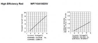
5V across a white LED is enormous.
It will blow up.
5V across a red LED is even worse. It will blow up approximately ten times as fast.
There is something in the datasheet that you don't understand and thus end up posting a misleading pair of graphs.
Those graphs DO NOT depict the Vf of a RED LED.
It will blow up.
5V across a red LED is even worse. It will blow up approximately ten times as fast.
There is something in the datasheet that you don't understand and thus end up posting a misleading pair of graphs.
Those graphs DO NOT depict the Vf of a RED LED.
Last edited:
Go and look at fig7 of VOM1271 datasheet.
Now compare to this line in the Knightsbridge datasheet.
Now compare to this line in the Knightsbridge datasheet.
if you are going to try designing anything electronic you need to learn how to read a datasheet.5V internal resistor.
Last edited:
This LED has nothing to do with the VOM1271. Yes, I have examined Fig 7 of the VOM1271 and that's why I adjusted the Vf in the for the proxy diodes used for the VOM1271 in the .asc to 1.44V.
Quite separately, there is the use of an LED - for which I have the WP710A10ID5V - between the 5V supply and the FPO pin of the TPS3510. I have provided a link to the data sheet for this LED repeated here. Tell me how I am misreading this data sheet.
You keep repeating my question back to me. I'm asking how to read this data sheet correctly and whether for this particular LED and a 5V supply I need a (further) resistor and, if so, how big should it be. It would seem to me the answer is "no" but you have said you disagree.
is on the 7th line of the intro to the datasheet.5V internal resistor.
Read it !
I read it. In responding in post 213 you likely didn't.
I was asking for confirmation of my reading of the data sheet including the line you now repeat. You responded that Vf of 5V would blow the LED and that I had posted misleading extracts from the data sheet (alongside a link to the full data sheet). Perhaps you should have responded along the lines of:
"Yes your reading of the data sheet is correct. While normally a Vf of 5V would blow a red LED, the WP710A10ID5V incorporates an internal resistor and so, as you indicate, there's no need for a further current limiting resistor with a 5V supply."
A Vf = 5V is nonsense.
You seem unable to understand that 5Vf will blow up a LED.
The plot you posted is {Vf+Vr} Get it?
I should not have to download your links to show you, that you cannot read and have posted misleading information.
My post213
You seem unable to understand that 5Vf will blow up a LED.
The plot you posted is {Vf+Vr} Get it?
I should not have to download your links to show you, that you cannot read and have posted misleading information.
My post213
is correct.5V across a white LED is enormous.
It will blow up.
5V across a red LED is even worse. It will blow up approximately ten times as fast.
There is something in the datasheet that you don't understand and thus end up posting a misleading pair of graphs.
Those graphs DO NOT depict the Vf of a RED LED.
Last edited:
Andrew, the reason why I asked the question in the first place was because I thought a Vf of 5V was extremely high. And yet, everywhere in the data sheet including the charts I extracted it only mentioned Vf - not Vf +Vr. For example, the plot I posted is labelled "forward voltage". I posted the data sheet which was exactly what I was asking for help in interpreting - to say I posted misleading information is nonsense. As it was somewhat confusing I asked for simple confirmation. Now, you say "a Vf = 5V is nonsense" despite it being provided repeatedly in the data sheet I provided. It would appear that a Vf of 5V for the device isn't because of the internal resistor. I had asked about the device, the thing I have purchased, not any old red LED.
Thanks for your help.
Thanks for your help.
- Status
- This old topic is closed. If you want to reopen this topic, contact a moderator using the "Report Post" button.
- Home
- Amplifiers
- Power Supplies
- Enough current to turn on 3 mosfets?