SGK,
Remove C1, C2, C3.
Paul
I took another look at the calculations for these and it would indeed seem possible to remove them. The guided to capacitive loads that need to be handled are 8,000uF for 12V and 6,000uF for the 5V and 3V3 respectively. The SOA of the IRFS7437pbF is:
An externally hosted image should be here but it was not working when we last tested it.
If we use Mark's calculations from post 95 but with these capacitive loads and a more conservative 10msec ramp up, even the 12V rail would seem to be okay - assuming I have done things correctly. Inrush = 0.008 x 12 / 0.01 = 9.6A. This is well inside the 10msec SOA curve. (A longer ramp up would mean less current rush.) If I have made a mistake in judgement here hopefully Mark will challenge my thinking! He might say something like "for the sake of one little capacitor would it not make sense to protect the pass transistor at a level well above the desired operating spec of 5A yet comfortably below the SOA limit" but then one is back trying to estimate the current provided by the VOM1271 to charge the cap from Mosfet gate to ground.
Last edited:
I suggest you read post #27 again. It said,... but then one is back trying to estimate the current provided by the VOM1271 to charge the cap from Mosfet gate to ground.
If you discard photovoltaic optoisolators, and if you confine yourself to BJTs, JFETs, MOSFETs, resistors, capacitors, diodes, ICs, and inductors, these are native elements in LTSPICE. Which means that you can try out your circuit design in simulation and see, with your own eyes, exactly how well it performs. If adequate, rejoice. If not adequate, redesign and resimulate.
One way to do this is shown below.
It discards ten of your circuit elements (U1, U2, U3, C1, C2, C3, R5, R6, Q1, Q2) and replaces them with fourteen new circuit elements (3xNMOS, 4xResistor, 3xCapacitor, 3xDiode, 1xIntegratedCircuit).
The circuit can be simulated and indeed I simulated it myself, this morning, between coffee and shower. (LTSPICE simulation .asc files attached).
It is powered from the +12V input supply and consumes 250 milliwatts.
Please note that the Schottky diodes and the NMOSFETs are available as "duals" with 2-in-a-package.
_
Attachments
SGK,
You could model the entire turn on sequence. Attached is a model of the vom1271 (but only accurate for 20mA of LED current) that I created some time ago. See the instructions in the zip file. Hopefully you will have a model for the mosfet.
Regards,
Paul Bysouth
You could model the entire turn on sequence. Attached is a model of the vom1271 (but only accurate for 20mA of LED current) that I created some time ago. See the instructions in the zip file. Hopefully you will have a model for the mosfet.
Regards,
Paul Bysouth
Attachments
Thanks Mark. Thanks Paul.
Mark, as much as I'd like to start again I think that's a bit too much work for what would appear an unlikely problem. The data sheet for the VOM1271 provides good guidance for typical short circuit current for a given IF; only component tolerances make this imprecise and if I have done my calculations correctly I have a reasonable amount of headroom to play with. It would appear easy to conclude there's no issue with the 3.3V and 5V (although I will leave room for caps on the board; why not). Now the 12V...
I set myself an arbitrary spec of 5A capability. A very rough interpolation of the IRFS7437 SOA chart suggests it can sustain at least 10A for 10msec. The ATX Power Supply Design Guide sets guidance for capacitive load of 8,000uF for 12V power rail. (There may be some headroom there as well.) On the basis of:
Imax = Cload x Ipu / Cgate
where Ipu is the current charging the gate capacitance of the pass transistor, ignored, and Cgate (Cgate connected from gate to ground)
and IF = 20mA => Isc = 30uA (from VOM data sheet)
(just to use something closer to the mid-point of the VOM1271 current capability)
then Cgate = 33nF slots things roughly down the middle of the current range above.
If, for whatever reason, Isc is closer to 20uA then Imax will be closer to 4.8A. If for any reason, Isc is closer to 40uA then Imax will be closer to 9.7A. If all other things are typical except Vf for the VOM LED, then Isc 40uA => IF = approx 26mA (interpolating the info on the VOM data sheet) which means all 3 of the VOM need to be at around Vf of 1.33V versus their typical 1.4V+ (Fig 7 VOM1271 data sheet; 25C). Now maybe that boils down to very little room for manoeuvre across three VOMs and maybe I get unlucky. If I blow a pass transistor I will replace it and double Cgate.
So that leaves determining the value of R6. Using a basic diode model to simulate three diode drops of 1.42V each suggests 34.8 Ohms would be good for R6.
If I am making a fatal error in judgement/calculation please let me know.")
Paul, thanks for the VOM1271a model. It's going to take me a little fiddling to get it to work as your .subckt file includes a reference to a fixed place on your computer. There's also a call on .lib PC817.sub. (Each highlighted in red below.) I thought it unusual to have to call up libraries within .subckt statements. (I use a Mac at home and so it's not as easy as placing the files in installation-dependent directories. Better to have all required files in the folder with the schematic in question.)
** vom1271 v3 subckt
** 20mA LED current
**
.subckt vom1271 1 2 3 4
E1 4 N002 N001 2 435000
R3 3 N002 290k
XU1 1 N001 NC_01 N001 PC817 Igain=2.3m
J1 4 N002 3 BF862
R1 N001 2 1m
.model NJF NJF
.model PJF PJF
.lib C:\PROGRA~2\LTC\LTSPIC~1\lib\cmp\standard.jft
**
.model JBF862 NJF(Beta=47.800E-3 Betatce=-.5 Rd=.8 Rs=7.5000 Lambda=37.300E-3 Vto=-.57093
+ Vtotc=-2.0000E-3 Is=424.60E-12 Isr=2.995p N=1 Nr=2 Xti=3 Alpha=-1.0000E-3
+ Vk=59.97 Cgd=7.4002E-12 M=.6015 Pb=.5 Fc=.5 Cgs=8.2890E-12 Kf=87.5E-18
+ Af=1)
***
.lib PC817.sub
**
.ends vom1271
Mark, as much as I'd like to start again I think that's a bit too much work for what would appear an unlikely problem. The data sheet for the VOM1271 provides good guidance for typical short circuit current for a given IF; only component tolerances make this imprecise and if I have done my calculations correctly I have a reasonable amount of headroom to play with. It would appear easy to conclude there's no issue with the 3.3V and 5V (although I will leave room for caps on the board; why not). Now the 12V...
I set myself an arbitrary spec of 5A capability. A very rough interpolation of the IRFS7437 SOA chart suggests it can sustain at least 10A for 10msec. The ATX Power Supply Design Guide sets guidance for capacitive load of 8,000uF for 12V power rail. (There may be some headroom there as well.) On the basis of:
Imax = Cload x Ipu / Cgate
where Ipu is the current charging the gate capacitance of the pass transistor, ignored, and Cgate (Cgate connected from gate to ground)
and IF = 20mA => Isc = 30uA (from VOM data sheet)
(just to use something closer to the mid-point of the VOM1271 current capability)
then Cgate = 33nF slots things roughly down the middle of the current range above.
If, for whatever reason, Isc is closer to 20uA then Imax will be closer to 4.8A. If for any reason, Isc is closer to 40uA then Imax will be closer to 9.7A. If all other things are typical except Vf for the VOM LED, then Isc 40uA => IF = approx 26mA (interpolating the info on the VOM data sheet) which means all 3 of the VOM need to be at around Vf of 1.33V versus their typical 1.4V+ (Fig 7 VOM1271 data sheet; 25C). Now maybe that boils down to very little room for manoeuvre across three VOMs and maybe I get unlucky. If I blow a pass transistor I will replace it and double Cgate.
So that leaves determining the value of R6. Using a basic diode model to simulate three diode drops of 1.42V each suggests 34.8 Ohms would be good for R6.
If I am making a fatal error in judgement/calculation please let me know.
Paul, thanks for the VOM1271a model. It's going to take me a little fiddling to get it to work as your .subckt file includes a reference to a fixed place on your computer. There's also a call on .lib PC817.sub. (Each highlighted in red below.) I thought it unusual to have to call up libraries within .subckt statements. (I use a Mac at home and so it's not as easy as placing the files in installation-dependent directories. Better to have all required files in the folder with the schematic in question.)
** vom1271 v3 subckt
** 20mA LED current
**
.subckt vom1271 1 2 3 4
E1 4 N002 N001 2 435000
R3 3 N002 290k
XU1 1 N001 NC_01 N001 PC817 Igain=2.3m
J1 4 N002 3 BF862
R1 N001 2 1m
.model NJF NJF
.model PJF PJF
.lib C:\PROGRA~2\LTC\LTSPIC~1\lib\cmp\standard.jft
**
.model JBF862 NJF(Beta=47.800E-3 Betatce=-.5 Rd=.8 Rs=7.5000 Lambda=37.300E-3 Vto=-.57093
+ Vtotc=-2.0000E-3 Is=424.60E-12 Isr=2.995p N=1 Nr=2 Xti=3 Alpha=-1.0000E-3
+ Vk=59.97 Cgd=7.4002E-12 M=.6015 Pb=.5 Fc=.5 Cgs=8.2890E-12 Kf=87.5E-18
+ Af=1)
***
.lib PC817.sub
**
.ends vom1271
I guess if it burns out components you can always re-layout the board with a larger percentage of "value is not yet decided" components, including value=Zero and value=Infinity. Then horse around in experimentation.
Resistor=Zero is the same as Capacitor=Infinity.
Resistor=Infinity is the same as Capacitor=Zero.
You can derive more sooth-sayings if you desire.
Resistor=Zero is the same as Capacitor=Infinity.
Resistor=Infinity is the same as Capacitor=Zero.
You can derive more sooth-sayings if you desire.
well I am hoping it's not a case of completely unknown. The necessary typical values are provided in the datasheet. It's just a matter of whether there are variances from typical that don't get averaged out across the 3 VOM. (Even native elements in LTspice can vary from 'typical'', right?) I guess that in a circuit which requires protection elements one would prefer to rely on parts with less potential device variance but as mentioned it would seem there's good headroom in the pass transistor SOA to begin with. Hopefully I haven't screwed up any other bits of the circuit/measurement pre-amp/board layout!
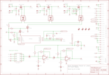
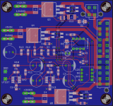
Hopefully almost there. Schematic, board and BoM attached. Any comments/suggestions welcomed.
(I'm getting nervous ahead of sending it to the board house and ordering parts from Mouser.)
(I'm getting nervous ahead of sending it to the board house and ordering parts from Mouser.
)Attachments
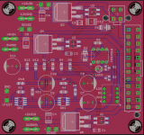
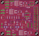
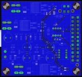
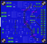
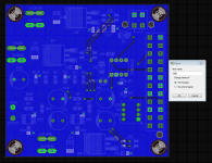
Ground 'planes' and copper pours.
The discussion of this topic in my PSU thread made me revisit this subject in relation to this board. My presumption is that while there aren't rectification pulse currents to deal with, the subject of a good/decent ground scheme remains important.
The attached two images attempt to show the bottom (blue) and top (red) ground 'planes' I have deployed until now. In each case the GND pour is highlighted as are the pads or pins connecting to GND (either blue or red and lime green respectively).
Peufeu would likely suggest the top pour is pointless given how dissected it is. Even the bottom layer is heavily dissected by the bottom layer traces.
I presume the board would benefit from, at a minimum, some vias connecting top and bottom pours near the ground connections of the SMD parts. Perhaps some jumpers would be required to cross the 'railway tracks' on the bottom layer. Other enhancements may well take a decent amount of rework.
Before I embark on this I wanted to check if I am barking up the wrong tree and ask if there were other considerations I should take into account.
Regards
Steve
Attachments
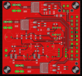
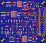
Thanks. I did my best to improve things without jumpers but your top two suggestions are still likely recommended. I removed the top pour, grounded SMD parts directly to the bottom layer with vias or connections to large nearby through-hole components. I also did a bit of rerouting and reduced the width of low-current connections to 16 mil. (Still exccessive but I don't have the confidence to route between the pads of a 1206 resistor and so thinner ones are of little benefit that I can see.)
Any guidance as to wire to use for the jumpers and is there a convention with respect to how to mark the board for such?
Any guidance as to wire to use for the jumpers and is there a convention with respect to how to mark the board for such?
Attachments
Most people just use off-cuts from trimming the leads of diodes, resistors, and capacitors. #22AWG or thereabouts.
A jumper is a two terminal component ("schematic symbol"). Designers happen to use them such that the two terminals often get wired to the same node. Footprint is usually just a straight line on top silkscreen with Jnnn for a part designator. If you've got jumpers of length 0.4", 0.7", and 0.8" you might make three footprints, one for each length.
Sometimes I tell the schematic it's a 1/4 watt thru hole resistor and use that footprint, if the lead spacing is okay and the width doesn't interfere with other topside components. Now I can use automatic board stuffing machines and reels of "Zerohm" resistors.
Ok that was rather obvious in hindsight - standard parts in Eagle. J1 and J2 added. The jumpers have 0.81mm drill holes and 1.6mm wide octagonal pads and I think I have some 0.6mm solid core hook up wire.
Hopefully now I just need to generate and edit the silk screen and then send it off.
Hopefully now I just need to generate and edit the silk screen and then send it off.
Attachments
Perhaps a little too much solder on the SOT-23 pins but otherwise it would seem my "skillet" soldering went ok. Soldering the GND pins of the through-hole parts was much more difficult (due to the large GND plane). The glue temporarily holding the pins made a little mess. I need to make a little jig or something for these things.
I hope I didn't make any mistakes populating the board! I wish I had a bench supply in order to hook up the three voltages and test it...
I hope I didn't make any mistakes populating the board! I wish I had a bench supply in order to hook up the three voltages and test it...
An externally hosted image should be here but it was not working when we last tested it.
Very nice job, especially the solder fillets on the tabs of the big honking MOSFETs!
I think if it were my board, I'd try to dribble in just a little bit of solder on the component side of the six high power blade connectors -- just for cosmetic appearance of Mega Ampere Capable.
I think if it were my board, I'd try to dribble in just a little bit of solder on the component side of the six high power blade connectors -- just for cosmetic appearance of Mega Ampere Capable.
Thanks. I almost blew it when I picked the board off the 'skillet' because those Mosfets were floating on a pool of solder which hadn't yet cooled enough to resist their weight.
I will add the solder on the blade connectors.
(The power rail board has a couple of 0805 caps on it. They will be another step up in terms of 'small'.)
I will add the solder on the blade connectors.
(The power rail board has a couple of 0805 caps on it. They will be another step up in terms of 'small'.)
Last edited:
- Status
- This old topic is closed. If you want to reopen this topic, contact a moderator using the "Report Post" button.
- Home
- Amplifiers
- Power Supplies
- Enough current to turn on 3 mosfets?