Corporation audio activities in pictures
Audio came from the mixer, line and microphone are mixed, hit hat was captured by microphone:
YouTube - Audio amps, Dx Corporation pictures
Audio came from the mixer, line and microphone are mixed, hit hat was captured by microphone:
YouTube - Audio amps, Dx Corporation pictures
Last edited:
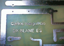
Well, congratulations Carlos, for some fine Quality Control checking. I'll be working on v1.4 today. I'm so ashamed. The DX Shameful.
It's becoming obvious that learning & using PCB layout software is the only way I (or anyone) should be creating board layouts. (Unless and until Adobe adds a ratsnest feature to Illustrator to correlate pads with a schematic -- doubtful.)
..Todd
It's becoming obvious that learning & using PCB layout software is the only way I (or anyone) should be creating board layouts. (Unless and until Adobe adds a ratsnest feature to Illustrator to correlate pads with a schematic -- doubtful.)
..Todd
It is all rigth dear Todd, i use to make several mistakes each day, in the reality
we all do such kind of things, some of us are too much arrogant to see this, others are more connected to reality and use to observe themselves with some critic eye.
This work, produce boards, this show us clearly how many errors we can do, also building amplifiers, it is very frustrating for us, for sure it is terrible as we face ourselves, our human side, that is different than our own self steem and pride.... the giant Ego we all have.
We see how many failures we can make, wrong decisions, things we do not see and they are in front of our eyes.
This makes us more humble, this is evolution, we learn, because of that knowledge applyied to our daily lives, not to ask too much from others, as we are also. something not very special... we fail, them can fail too.
I am proudfull of you, different than shamefull, you are busy, have a lot to do, wife, daddy, mum, work, and even this way you do not forget your responsability with your friends.
Because i know that, many years ago i have learned how bad i can be producing boards and building, destroying part, exploding amplifiers, ....it is because of that i am demanding with people that offer to produce boards...i use to say, do not make boards if you do not intend to build to test your piece of trouble!..... this is because i recognize, that not only me, we all do mistakes.
To tell you the truth, even here in this forum i am watching several people doing mistakes, the only one i could not see doing this kind of thing was my beloved and prefered moderator..but one day he will fail too, he is human.
Our moderator's crew are wise, they do not like to make intervenctions, reducing that they reduce their tax or errors too..very clever they are... when we, humans, when we move, there's a big chance to be unfair, to make bad judgment.... the old buddy, the mistake, is always waiting a a chance to attack us again.
We start to make mistakes early morning, we do not brush our teeth in the first moment, we do not say good morning with a tender hug to our wife and sons..we run because we have no time.... this is not correct, go increasing distance between daddy and family...loosing important moments to say to our lovely ... to say " i love you"... time passes, they grow up and leave us, our wife become old and sick and we have lost valuable moments to make them know you love them.
Congratulations dear Taj, i know how busy you are.
regards,
Carlos
Last edited:
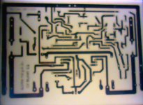
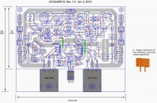
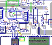
New PCB files: v1.4 attached.
- VAS connections fixed
- VBE multiplier resistor connection fixed
- More pad spacing for TO-92 and TO-126 transistors
- more track spacing in tight spots
- Added [optional] output coil footprint (and instructions)
Attachments
One more building, Danilo e building using his own eagle designed board
It is very popular to use hot iron transference of toner to the board here.
People prepare layout and then they produce laser printer copies, then they attach the toner image against the board, copper side touching the toner, last movement is to apply heat using hot iron, these ones we use to our pants and shirts when they come out from the washing machine.
The toner melt and is transfered to the copper board side alike a rubber track, this protects against the corroding acid we use (Percloreto de Ferro), the board can go to the corroding bath.
To remove the paper, we let it under the water and we use finger points to remove completely before go to the acid to corrosion.
Result is never very good, we also use to paint the board with photo sensitive material and to transfer the image using the layout printed in a transparency film, the tracks are transparent, them we apply strong light that crosses de transparent tracks and go to the photo sensing chemical material..this works better but is expensive and the chemical product is not easy to find.
We do not use to order boards in small numbers, the cost is too high for our brazilian standards.
I have tried to fix something in the left image, some letters were missed because the hard corrosion the board has suffered.
regards,
Carlos
Attachments
Marcisio, our Thai Box champion, has printed a very big image from the pcboard
to give it a triple check.
He lives in Pará State, very near the Amazon river and Amazon jungle, he is a cyber Policeman, searching for internet crimes.
Dx Corporation is constituted by people, they have family, they have faces and pictures to show, also the crew members are this way.
regards,
Carlos
Attachments


Last edited:
![P1030[01]_05-01-10.jpg](/community/data/attachments/161/161772-4b672a7c6628f584214a82a163fdd464.jpg)
Great!.....nice!... thank you Andrewlebon
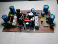
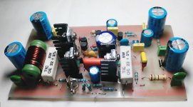
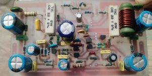
Nice pictures, good resolution, good light, nice focus, pretty boards and LOVELY amplifier.
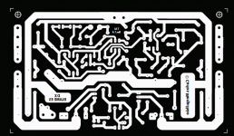
I will be here to help, you know we have the pcboard version 1.4, also the layout version 1.4, several things found wrong, a friend using version 1.0 is having hard time searching for our mistakes, in the circuit, and also in the layout.
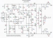
I suggest you, deeply, to INSPECT carefully your board, against strong light, and follow each copper trace and track, draw the checked lines into a schematic you have previously printed, then go painting, or drawing all lines in red to be sure everything is connected and no short or missed things are there.
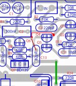
Check your transistor leads several times, BC546 and BC556 have the base in the middle, it is different compared to the traditionally used 2N5401 sand 2N5551, these were not used as voltage is very small, simulators shows almost the same result with one or other, also listening tests have not show audible, listenable differences.
There's important capacitors, cannot forget these ones, the second VAS, the BD139 colector to ground (470pf), the CCS base to coletor (100pf) and the compensation capacitor (82 or 100pf) from second vas coletor to first Vas base.
Current, in stand by mode, must be adjusted from 30 to 100 miliamps, and 44 miliamps is what i am using with nice results and excelent simulation, this keep a good current crossing the power output transistors, each one of them will dissipate 1 watt.
Of set, usually goes to 14 miliamperes, the 1K resistance, or 1K2 resistance, in parallel with R68 should be used if really needed, you may tollerate off set till 25 miliamperes without bother with off set... good forum engineers told this is something may unstabilize, so, better not to use, unless hardly needed.
I am here to help, if needed.
regards,
Carlos
Nice pictures, good resolution, good light, nice focus, pretty boards and LOVELY amplifier.
I will be here to help, you know we have the pcboard version 1.4, also the layout version 1.4, several things found wrong, a friend using version 1.0 is having hard time searching for our mistakes, in the circuit, and also in the layout.
I suggest you, deeply, to INSPECT carefully your board, against strong light, and follow each copper trace and track, draw the checked lines into a schematic you have previously printed, then go painting, or drawing all lines in red to be sure everything is connected and no short or missed things are there.
Check your transistor leads several times, BC546 and BC556 have the base in the middle, it is different compared to the traditionally used 2N5401 sand 2N5551, these were not used as voltage is very small, simulators shows almost the same result with one or other, also listening tests have not show audible, listenable differences.
There's important capacitors, cannot forget these ones, the second VAS, the BD139 colector to ground (470pf), the CCS base to coletor (100pf) and the compensation capacitor (82 or 100pf) from second vas coletor to first Vas base.
Current, in stand by mode, must be adjusted from 30 to 100 miliamps, and 44 miliamps is what i am using with nice results and excelent simulation, this keep a good current crossing the power output transistors, each one of them will dissipate 1 watt.
Of set, usually goes to 14 miliamperes, the 1K resistance, or 1K2 resistance, in parallel with R68 should be used if really needed, you may tollerate off set till 25 miliamperes without bother with off set... good forum engineers told this is something may unstabilize, so, better not to use, unless hardly needed.
I am here to help, if needed.
regards,
Carlos
Attachments
Last edited:
Dc Corporation follow up division, also Art and layout division will be working
during group vacations,
Marketing department will operate half period
Laboratories A and B are closed till february, people is walking along the beach... and this was the biggest bikini i could find there!... i really do not know if the bikini is too much small or.........................................
No copies, research, construction of prototypes or modules, also no dirty spy cloning activities running those next days.
attached the laboratory "B", disabled for a while and the hot toner image transfer layout
regards,
Carlos
Attachments

Last edited:
Nice pictures Andrewlebon
I have made them bigger to allow better forum image zooming.
diy customers support department will provide around clock follow up
You are not using last boards, there are errors in this one... i hope you know them, in the input, and also in the VBE multiplier
regards,
Carlos
I have made them bigger to allow better forum image zooming.
diy customers support department will provide around clock follow up
You are not using last boards, there are errors in this one... i hope you know them, in the input, and also in the VBE multiplier
regards,
Carlos
Attachments
Last edited:
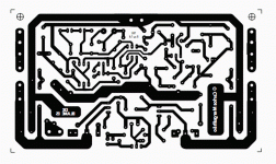
Attention Andrewlebon!
There are errors that were fixed in the version 1.4 layout
here the images used to inform Todd that we had these errors, they are now fixed, but i am afraid your board have these errors, as your boards seems to me not to be version 1.4.
So, you have tracks to cut and wire jumpers to solder.
regards,
Carlos
Attachments
dx blameless
dear sir
greetings thank you for the encouragement .I am using 1.1 version
have put 470 pf 100pf 82 pf there is one condenser 100uf 16 volts on pcb
layout but schematic does not show it should i remove it any power supply
tips yes i will check pcb with schematic before powering on.Once again
thank you will inform you of the results
thanking you
andrew lebon
Check everything before power the unit on, those former boards
1.0, 1.1, 1.2 and 1.3 have errors, so, you must check everything.
The one you do not need to check is 1.4, this one three friend and me have checked, the chance to have remaining errors are very small, but it is not impossible to have errors, ship happens!
Wait for a perfect ballanced sound, with the highest possible quality in the high frequencies, the best audio amplifier i have ever listened.
But, i think the bass is shy, yeah, not my boomy head taste, the Dx amplifier produces much more loosen deep hell bass.
Watch this video, the sound is more to Dx Amplifier than to Dx Blame ES.
A matter of taste, personnal preferences..the best is the Dx Blame ES, but the best bass to my taste goes to the Dx Standard.
YouTube - Subwoofer Hinor Impact 15' quebrando CD (segundo video)
regards,
Carlos
.......................................................................
Check everything once, check twice and check once more watching the schematic and painting track lines in red or other colour, print the 1.3 schematic and check everything prior to power the unit on.
To the ones loves pictures too
Dx Corporation pictures II:
YouTube - Audio amps, Dx Corporation pictures 2
Dx Corporation pictures II:
YouTube - Audio amps, Dx Corporation pictures 2

") ) maybe.
) maybe.- Status
- This old topic is closed. If you want to reopen this topic, contact a moderator using the "Report Post" button.
- Home
- Amplifiers
- Solid State
- Dx Blame ES .... based into the Blameless, i am trying a new amplifier