crossover distortion
I suggest a test for evaluating crossover distortion. The amp (DUT) being tested is connected as usual with the AP S1. Reading output of S1 is the signal from the analyzer section. When the analyzer is doing Amplitude measurement, Reading output is basically scaled S1 input signal or the amp output.
The AP S1 Reading output feds a Class-A or headphone amp with volume control. Note the Reading output is not low noise. Set a listening level (volume control) for a test tone, say, 1 kHz (Analyzer measuring Amplitude). I make it SLP = 84 dB for 1 m from the speaker. Set the bias of the DUT to lowest which causes severe crossover distortion. Now switch the Analyzer to THD+N Ratio mode. The Reading output is now the THD+N residual. We can hear the distortion clearly due to strong crossover spikes.
The bias is now gradually increased. For instance increased to the bias level for THD+N = 0.0009 %, can we hear anything beside the notched fundamental? Although the crossover harmonics are below 90 dBV (FFT in earlier threads), I still can hear the harmonics easily. The sound level meter shows 51 dB. When the bias is further increased to 22 mA per device, I can't hear anything but hiss noise. The sound level meter reading is 49 dB.
try grossly under-biasing your ClassAB amp and play back music with an average level of 20dB to 30dB below maximum power.
I suggest a test for evaluating crossover distortion. The amp (DUT) being tested is connected as usual with the AP S1. Reading output of S1 is the signal from the analyzer section. When the analyzer is doing Amplitude measurement, Reading output is basically scaled S1 input signal or the amp output.
The AP S1 Reading output feds a Class-A or headphone amp with volume control. Note the Reading output is not low noise. Set a listening level (volume control) for a test tone, say, 1 kHz (Analyzer measuring Amplitude). I make it SLP = 84 dB for 1 m from the speaker. Set the bias of the DUT to lowest which causes severe crossover distortion. Now switch the Analyzer to THD+N Ratio mode. The Reading output is now the THD+N residual. We can hear the distortion clearly due to strong crossover spikes.
The bias is now gradually increased. For instance increased to the bias level for THD+N = 0.0009 %, can we hear anything beside the notched fundamental? Although the crossover harmonics are below 90 dBV (FFT in earlier threads), I still can hear the harmonics easily. The sound level meter shows 51 dB. When the bias is further increased to 22 mA per device, I can't hear anything but hiss noise. The sound level meter reading is 49 dB.
Last edited:
Hi Panson,
Thanks for the plots, I'm still jealous of your AP-1. I don't think I can remove the fundamental with RMAA. I ran my simulation of a similar configuration, which has a "perfect" front end to represent the 49811. The schematic is attached. I didn't calculate the RMS output, just took a swag at it with 50v supplies and 45v signal (which represents the signal voltage coming from the VAS - in this case the 49811). The FFT output is quite similar to your measured results - I drew a line at the -110db level to represent your noise floor. I think you can see that the harmonic content and amplitudes are consistent between the simulation and the actual amp. I also printed the predicted Thd numbers again quite close to your measured .0003 number.
Ken
Ken,
You can consider to make an active notch filter (e.g. 1 kHz) to reject the fundamental to improve your measurement power.
Your output stage in the simulation is open-loop. Is it what you do in hardware? You may put an op-amp to your model to represent the front end and close the loop.
Panson
Hi Panson,
I'm still jealous of your AP-1.
Ken
The AP is indeed a powerful equipment. It allows us to do check many things in details. My one is from eBay - a good investment.
Ken,
You can consider to make an active notch filter (e.g. 1 kHz) to reject the fundamental to improve your measurement power.
Your output stage in the simulation is open-loop. Is it what you do in hardware? You may put an op-amp to your model to represent the front end and close the loop.
Panson
Hi Panson,
Do you remove the fundamental before the DUT or after the DUT?
Ken
Hi Panson,
Do you remove the fundamental before the DUT or after the DUT?
Ken
After the DUT, before the FFT (or your sound card).
Thermal tracking exercise
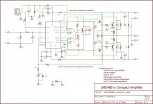
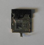
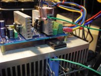
Here are some data collected recently for thermal tracking. The schematic is shown below for reference. Middle picture shows a TT with package removed. How thermalcoupler attached to the heatsink is shown in the right picture.
Initial bias target was 22 mA (~5 mV across Re R3/R4). NPN side was measured. For Case 3, both N and P of TT BE and diode were measured. The P side is consistent with the N side.
Case 1: R12 and R22 shorted.
Over-bias is due to driver Vbe decrement. We might increase the TT diode tempco. Here, I take another approach by tracking the driver temperature.
Case 2: a MJE15030 "diode" inserted at R12 and mounted on the driver heatsink.
Over-bias issue is slightly mitigated by using the "diode" to partially compensating the BE tempco.
Case 3: two MJE15030 "diodes" inserted at R12 and mounted on the driver heatsink
Over-bias issue is further mitigated by using two "diodes". Further improvement is still needed.
Comment please.
Here are some data collected recently for thermal tracking. The schematic is shown below for reference. Middle picture shows a TT with package removed. How thermalcoupler attached to the heatsink is shown in the right picture.
Initial bias target was 22 mA (~5 mV across Re R3/R4). NPN side was measured. For Case 3, both N and P of TT BE and diode were measured. The P side is consistent with the N side.
Case 1: R12 and R22 shorted.
Main heatsink: 21 C, Driver heatsink: 24 C
Re 5.1 mV
TT diode 559.4 mV
TT BE 577.1 mV
Driver BE 576.7 mV
pot 1.188 V (voltage across pot R20)
TT diode 559.4 mV
TT BE 577.1 mV
Driver BE 576.7 mV
pot 1.188 V (voltage across pot R20)
Main: 55 C, Driver: 43 C
Re 35.8 mV
TT diode 471.3 mV
TT BE 521.8 mV
Driver BE 519.2 mV
pot 1.188 V
TT diode 471.3 mV
TT BE 521.8 mV
Driver BE 519.2 mV
pot 1.188 V
Over-bias is due to driver Vbe decrement. We might increase the TT diode tempco. Here, I take another approach by tracking the driver temperature.
Case 2: a MJE15030 "diode" inserted at R12 and mounted on the driver heatsink.
Main: 19 C, Driver: 22 C
Re 5.6 mV
TT diode 562.1 mV
TT BE 580.8 mV
Driver BE 582.5 mV
15030 diode 587.5 mV
pot 605.8 mV
TT diode 562.1 mV
TT BE 580.8 mV
Driver BE 582.5 mV
15030 diode 587.5 mV
pot 605.8 mV
Main: 54 C, Driver: 44 C
Re 23 mV
TT diode 480 mV
TT BE 525.8 mV
Driver BE 528.5 mV
15030 diode 536.5 mV
TT diode 480 mV
TT BE 525.8 mV
Driver BE 528.5 mV
15030 diode 536.5 mV
Over-bias issue is slightly mitigated by using the "diode" to partially compensating the BE tempco.
Case 3: two MJE15030 "diodes" inserted at R12 and mounted on the driver heatsink
Main: 27.5 C, Driver: 25 C
Re 6.0 mV
TT diode 546.5 mV
TT BE 563 mV
Driver BE 573.5 mV
15030 diodes 580.5 + 591 mV
pot 0
TT diode 546.5 mV
TT BE 563 mV
Driver BE 573.5 mV
15030 diodes 580.5 + 591 mV
pot 0
Main: 53.5 C, Driver: 39 C
Re 13 mV
TT diode 493.5 mV
TT BE 502 mV
Driver BE 536.5 mV
15030 diodes 549.5 + 559 mV
pot 0
TT diode 493.5 mV
TT BE 502 mV
Driver BE 536.5 mV
15030 diodes 549.5 + 559 mV
pot 0
Over-bias issue is further mitigated by using two "diodes". Further improvement is still needed.
Comment please.
Attachments
Last edited:
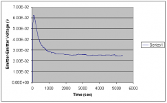
Panson: I agree, having the bias shift by 7x from turn-on to fully warmed up is an issue. My LME49811+STD03 amp changes from 27 mV across 0.44R at turn-on to 42 mV across 0.44R at fully warm. So 30-ish % change. Attached shows a bias measurement I took on a commercially available amplifier. This amp uses three pairs of output devices with 0.22R emitter resistors. I'm measuring from emitter to emitter from start-up of the amp and 90 minutes out. Just for reference.
The ON Semi devices, as you have verified, contain a separate diode and transistor mounted in one package. From your measurements, it seems the two have quite different tempcos. From your data (case 1), I calculate:
TT diode tempco = -2.59 mV/deg C
TT Vbe tempco = -1.63 mV/deg C
As the STD03 supposedly uses a diode that's integrated on the same die as the BJT, I would expect their tempcos to be identical but I haven't measured this. The STD03 is also 3~4x the cost of the ON Semi devices.
Anyway.... What to do about your circuit. You have three tempcos to keep track of: Drivers, output stage, and TT diodes. The drivers work out to be -1.54 mV/deg C - about the same as the output devices. But the TT diodes are quite different. Off the top of my head I don't see an easy way to change the tempco of the TT diode to match that of the output device. What would be interesting to try, though, is a Vbe multiplier using one of the driver devices mounted on the main heat sink. That kinda defeats the purpose of using the TT devices, but you should be able to get good performance, I'd think. In any event, your thermal sensor (TT diode or Vbe multiplier transistor) must be connected thermally to the main heat sink as the main output devices are the ones that need protection. Unless... Unless you use a CFP output stage (see Douglas Self's amp design book).
~Tom
Attachments
Anyway.... What to do about your circuit. You have three tempcos to keep track of: Drivers, output stage, and TT diodes. The drivers work out to be -1.54 mV/deg C - about the same as the output devices. But the TT diodes are quite different. Off the top of my head I don't see an easy way to change the tempco of the TT diode to match that of the output device. What would be interesting to try, though, is a Vbe multiplier using one of the driver devices mounted on the main heat sink. That kinda defeats the purpose of using the TT devices, but you should be able to get good performance, I'd think. In any event, your thermal sensor (TT diode or Vbe multiplier transistor) must be connected thermally to the main heat sink as the main output devices are the ones that need protection. Unless... Unless you use a CFP output stage (see Douglas Self's amp design book).
~Tom
Tom,
Yes, I will try Vbe multiplier later. Thanks for your advices.
Out of curiosity, I put the two 15030 diodes on the main heatsink, similar to your suggestion. Since the main heatsink is hotter than that of driver, I can effectively increase the overall bias tempco. It results in a very stable system. The Re drop varies from 5.x to 6.x mV.
Panson,
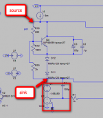
I keep going back to Cordell's solution to this issue. If you vary r19 and r20, you can tune the tempco of the TT diodes to match that of the output transistors. He has a chart for appropriate values for r19 and r20. If you're interested I can dig that up for you. Cordell suggests that the Vbe transistor be mounted on the same heat sink as the driver transistors to add a level of thermal tracking to the driver transistors. The mur120 diodes in the schematic represent the TT diodes for the amp.
Ken
Attachments
Panson,
I keep going back to Cordell's solution to this issue. If you vary r19 and r20, you can tune the tempco of the TT diodes to match that of the output transistors. He has a chart for appropriate values for r19 and r20. If you're interested I can dig that up for you. Cordell suggests that the Vbe transistor be mounted on the same heat sink as the driver transistors to add a level of thermal tracking to the driver transistors. The mur120 diodes in the schematic represent the TT diodes for the amp.
Ken
Ken,
Yes, please show me. Have you showed any result regarding thermal tracking (e.g. V across Re over time) in the forum?
Panson
Ken,
Yes, please show me. Have you showed any result regarding thermal tracking (e.g. V across Re over time) in the forum?
Panson
Hi Panson,
Here's the link: it's post 519 and 520
http://www.diyaudio.com/forums/solid-state/71534-semi-thermaltrak-52.html
I haven't done the level of measurement that you have. However, I have run the amp up to full output driven by a 1k sine wave into an 8 ohm load and found the bias to return to normal within about 1 to 1.5 seconds of removing the load. I just got a cheap hand held infra red temp sensor, so, I will try taking measurements and reporting back.
Ken
I measured my voltages as follows for the Cordell bias scheme with the 1.52 sensitivity - 3k/2,213 resistor combination:
Re resistors are 0R2
Main 30C
Re 5.5mv
TT diode 510mv
TT BE 594mv
Main 59 C
Re 6mv
TTdiode 465mv
TT BE 565mv
Ken
Ken
This is good!
Thank you for the links.
Panson
Ken
This is good!
Thank you for the links.
Panson
Panson,
Maybe to good... I didn't measure the Re correctly, don't know what I was thinking at the time, a bit embarassed here
 . Yesterday, I was doing other stuff and started to think, did I really put the probes there? I redo today and re-post.
Ken
so, back at it
First for my set up 12mv = about 22mA across Re's
with the 3k resistor in position R3
25C = 14mv
35.4C= 15mv
39.0C=17mv BE .542, TT diode .525mv
with 10k /931 (didn't have 893R)
29.4C=13mv
33.4C=16mv
35.0C=17mv
36.0C=17mv
37.0C=17mv
Seems the 10k/931 which has a lower sensitivity get quite stable. I will reset and try again tomorrow.
Ken
Ken,
Have you showed any result regarding thermal tracking (e.g. V across Re over time) in the forum?
Panson
Hi Panson,
I've compared my voltages across Re to the amperage across Re. My DMM say that 12mV = 22mA across two resistors each 0R2. The Ohm law calculator says that 22mA across 0r4 (2 x 0r2) = 8.8mV. Should I use the 8.8mV for setting the bias? Is there a better way the measure the resistance of the Re resistors for plugging into the calculation?
Thanks
Ken
I = V / R
V = I * R
R = V / I
Which is your unknown?
Choose the equation where the unknown is on the left most side.
Insert the two values that you know on the right most side. Solve.
V = 12mV = 0.012V
R = 0.22ohms.
Equation 1 is chosen since you know V & R
I = 0.012 / 0.2 = 0.06A = 60mA
V = I * R
R = V / I
Which is your unknown?
Choose the equation where the unknown is on the left most side.
Insert the two values that you know on the right most side. Solve.
V = 12mV = 0.012V
R = 0.22ohms.
Equation 1 is chosen since you know V & R
I = 0.012 / 0.2 = 0.06A = 60mA
- Home
- Amplifiers
- Chip Amps
- Compact Sized LME49810/11 +ThermalTrak Amp