Happened to be reading this .pdf and the Harris 2539 (page 23) reminds me of your design
a bit, note that the dual diff pair is driven directly:
https://web.stanford.edu/class/archive/ee/ee214/ee214.1042/Handouts/ho15opamp.pdf
Thanks for that! Indeed it is awfully similar. Shows there's nothing new in electronics.
I'm a huge fan of Lee. I reckon most things I know about RFIC design are straight out of his book "The design of CMOS RFICs". The book is worth buying for the "non-linear history of radio" chapter alone.
I haven't got the simulator in front of me, so this is pretty much off the top of my head.
I set the collector currents of the first diffamp to 1mA. R27 on Q17's emitter sources 2.5mA, of which 1mA goes to the first stage collector and the remaining 1.5mA is then available for the second stage. Base current for the second stage is assumed negligible, so most of this current flows through the cascode load R29, putting the second stage bases (and Q17 collector) at something like +9V with +/-18V supplies. This gives me 8V or so across Q17.
The choice of 18K for R29 limits my supplies somewhat, as it'll stop working under something like +/-14 or 15V.
So I guess in answer to your question, no, I didn't. I chose a lower voltage and am surprised it's that high. I'll have to recheck the bias conditions.
Hi BesPav,
I've been playing with bias conditions since I got home this evening in response to udok's comment. It's a tad more stable now, though my open-loop is only a rough approximation and lacks the rigour of what you're clearly doing:
I've been playing with bias conditions since I got home this evening in response to udok's comment. It's a tad more stable now, though my open-loop is only a rough approximation and lacks the rigour of what you're clearly doing:
Attachments
Hi Suzy,
I played with the compensation and it is stable now.
I have replace the TIP41 with modern D44H11.
The TIP41 has too low beta for your diamond buffers,
and limit the output swing.
In addition i did set the DC voltage of the first stage to near zero.
In the first longtail pair i added an inductor to bypass the emitter
degeneration resistors at audio.
THD at 1kHz is better than 120 dB, and better than 100 dB @ 10kHz
Greetings,
Udo
Attachments
Last edited:
Ok, i did some more minor tweaking of the compensation.
See the LTSpice file for details.
The inductor in the input longtail-pair is disabled to see a honest comparison
with the original design:
THD @ 1kHz better than 110 dB
THD @ 10kHz better than 90 dB
So the inductor brings about 10 dB.
See the LTSpice file for details.
The inductor in the input longtail-pair is disabled to see a honest comparison
with the original design:
THD @ 1kHz better than 110 dB
THD @ 10kHz better than 90 dB
So the inductor brings about 10 dB.
Attachments
Last edited:
Yes, the D44H11 are super.
The spice model from Harry Dymont is here:
https://dl.dropbox.com/s/v95mdjwit237sl5/transistor models.zip?dl=1
The spice model from Harry Dymont is here:
https://dl.dropbox.com/s/v95mdjwit237sl5/transistor models.zip?dl=1
I added a sim with a simpler and more capable CFB buffer stage:
THD@1kHz improves to 118 dB
THD@10kHz is now 109dB
With the inductor in the input stage switched on,
THD@10kHz is 121 dB
Open loop gain at 10kHz is 50 dB, and unity gain frequency is 3 MHz.
The output goes up to VCC - 2 Volt @ 8 Ohm load.
I will leave it now at this state.
Considering that the design has some serious drawbacks, i am surprised
how good it is finally.
This is mainly because of your 3 stage amplifier design!
Greetings,
Udo
Attachments
Last edited:
There isn't really. It's a sign of laziness on my part that the only net on the whole board that's manually named is GND. I didn't even name in, out, or power.
My CAD tool automatically assigns net names to every unnamed net, starting with N00001 and going up.
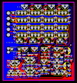
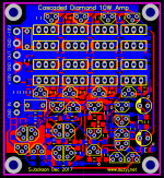
Something that I rather like about using through-hole parts (most all my layout these days is surface mount) is that I've almost always got a handy via to use, so there's a total of six vias on the whole PCB.
My CAD tool automatically assigns net names to every unnamed net, starting with N00001 and going up.
Something that I rather like about using through-hole parts (most all my layout these days is surface mount) is that I've almost always got a handy via to use, so there's a total of six vias on the whole PCB.
Hi Pete,
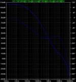
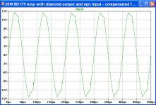
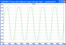
Yes, I have. It's dependent on load and compensation. For a 4 ohm load it's a tad ragged (see second trace), with a little bit of ringing. Wind the load back to 8 ohms and it's rather better behaved (first trace). I've included the sim file to show the exact compensation cap values used.
Yes, I have. It's dependent on load and compensation. For a 4 ohm load it's a tad ragged (see second trace), with a little bit of ringing. Wind the load back to 8 ohms and it's rather better behaved (first trace). I've included the sim file to show the exact compensation cap values used.
Attachments
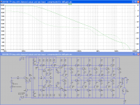
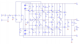
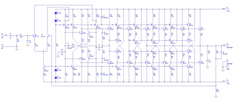
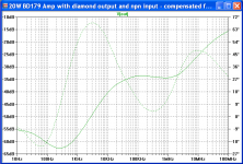
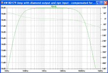
Possibly final schematic and layout for the 20W into 4 ohm (14W into 8 ohm) version, built with BD179 & BD180 transistors. I've put in provision for a DC blocking filter on the input. With 4K7 & 1u high pass is at ~35Hz. 4n7 on the diffamp base puts the low pass at ~170KHz.
I also threw a decent sized cap (100u 6V3) across each of the bias diode strings - that improves PSRR from ~55dB to ~60dB in the 100-800Hz region (shown). Plus I added components (not used at present) to allow me to add further compensation to the second stage, should that be useful - thanks Udo for that.
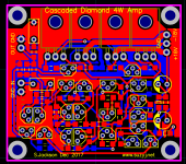
Finally, I've also knocked out a simpler 4W into 8 Ohms version - it's not terribly exciting, but it'll do <1ppm into 50 ohms, so should be a nice gain block for driving test instruments.
I also threw a decent sized cap (100u 6V3) across each of the bias diode strings - that improves PSRR from ~55dB to ~60dB in the 100-800Hz region (shown). Plus I added components (not used at present) to allow me to add further compensation to the second stage, should that be useful - thanks Udo for that.
Finally, I've also knocked out a simpler 4W into 8 Ohms version - it's not terribly exciting, but it'll do <1ppm into 50 ohms, so should be a nice gain block for driving test instruments.
Attachments
-
 Screen Shot 2017-12-16 at 10.33.09 pm.png509.3 KB · Views: 380
 -
 Screen Shot 2017-12-16 at 10.32.37 pm.png367.4 KB · Views: 257
 -
 Screen Shot 2017-12-16 at 10.31.38 pm.png524.9 KB · Views: 252
 -
 Screen Shot 2017-12-16 at 10.30.36 pm.png284.9 KB · Views: 218
 -
 Screen Shot 2017-12-16 at 10.29.03 pm.png186.7 KB · Views: 191
 -
 Screen Shot 2017-12-16 at 10.28.46 pm.png162.6 KB · Views: 148
Last edited:
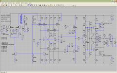
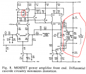
Since I am a huge fan of wretched excess, my version of this sort of amplifier (36V rails, many pairs of TO-126 "medium power" output transistors, etc) includes a number of extra components whose only purpose is to guarantee graceful clipping and graceful exit-from-clipping.
The basic concept is diagrammed in Bob Cordell's Error Correcting Power Amplifier paper {which you can download from his website}, Figure 1 below. All that stuff in red, exists only to guarantee graceful overload behavior.
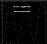
My implementation's simulated performance is in Figure 2 below. Full power bandwidth is quite decent. There's no "sticking to the rails" and there's no step function followed by ringing, when recovering from clipping. Compare to the figures in post #97.
I myself find the additional cost, for extra components, extra PCB area, and additional opportunities to make an assembly mistake, to be worthwhile. Others may find it wretched excess. Que sera sera.
Just wanted to point out that graceful clipping is readily achievable, Cordell's 1982 paper shows one way to do it, and I'm confident that several authors probably showed other ways to do it, even earlier.
_
The basic concept is diagrammed in Bob Cordell's Error Correcting Power Amplifier paper {which you can download from his website}, Figure 1 below. All that stuff in red, exists only to guarantee graceful overload behavior.
My implementation's simulated performance is in Figure 2 below. Full power bandwidth is quite decent. There's no "sticking to the rails" and there's no step function followed by ringing, when recovering from clipping. Compare to the figures in post #97.
I myself find the additional cost, for extra components, extra PCB area, and additional opportunities to make an assembly mistake, to be worthwhile. Others may find it wretched excess. Que sera sera.
Just wanted to point out that graceful clipping is readily achievable, Cordell's 1982 paper shows one way to do it, and I'm confident that several authors probably showed other ways to do it, even earlier.
_
Attachments
- Home
- Amplifiers
- Solid State
- Cascading diamond buffers - a cheap low THD 10W amp with TIP41C