Hi John,
"WS and DATA input signals were attenuated, each input, 3K3 to +5V, 1K to GND, and 3K3 from input to WS / DATA output. This significantly reduces HF interference being dumped on the DAC chip substrate."
at the moment I have 10 ohm resistors in series with the WS,DATA and BCK signals, please could you post a quick schematic of the above arrangement, just to be sure that I have got it down right. (10R to 3.3K seems like a big jump!)
I also have a couple of kits (pcbs and parts) that I intend to use for the I/V conversion on one of my diy TDA1541 DACs: please see attached file. I originally bought these kits from the diyparadise site for one of my other TDA1543 DACs and found them to sound better than my OPamp tube output I/V. From info provided in earlier posts I think they will be ideal for the TDA1541. - am I correct. I was going to use a seperate charge tfr power supply for around 20v plus Super regulators for this.
keep up the good work.
Attachments
cheers Jonners,
I think that the "less simple I/V circuit" is the way to go for the tda1541.
John,
quote: "WS and DATA input signals were attenuated, each input, 3K3 to +5V, 1K to GND, and 3K3 from input to WS / DATA output. This significantly reduces HF interference being dumped on the DAC chip substrate."
I would still like to see a schematic of the input attenuation scheme described above.
Brad
Re: charge transfer power and SPDIF
If I may ...
If this question is related to this project, you can't and besides you won't (it inherently just isn't bit perfect anymore).
Otherwise, find a digital output nearest to the DAC and loop it back for recording. Or use an internal loopback in the soundcard.
Then load the original and the recording in Wavelab, find a common start point in both files, and compare from there on.
If you can't find a common start point you'll have your answer too.
But maybe that is not what you wanted to know.
In either case this is about testing the software (player) for being bit perfect or not. You'll never be able to test the DAC for this. You could behind the receiver though, once it's not upsampling.
Peter
Onnosr said:Bit perfect SPDIF Question
---------------------------------
How are you measuring (comparing) bit perfect pass trough spdif.
(I know the DTS trick)
If I may ...
If this question is related to this project, you can't and besides you won't (it inherently just isn't bit perfect anymore).
Otherwise, find a digital output nearest to the DAC and loop it back for recording. Or use an internal loopback in the soundcard.
Then load the original and the recording in Wavelab, find a common start point in both files, and compare from there on.
If you can't find a common start point you'll have your answer too.
But maybe that is not what you wanted to know.
In either case this is about testing the software (player) for being bit perfect or not. You'll never be able to test the DAC for this. You could behind the receiver though, once it's not upsampling.
Peter
Hi ccschua,
By synchronizing the DEM (Dynamic Element Matching) clock with the master clock, you remove a free running (150 ... 250 KHz) high-jitter DEM clock source, preventing inter-modulation between DEM clock and master clock.
Note that ALL frequencies and harmonics, present in a DAC, WILL end up on your audio signal (crosstalk) and degrade / affect sound quality to some degree. This includes the DEM clock, word clock, master clock, data, power supply noise & hum, and (active) component noise, just to name a few of many. In fact, I2S interface crosstalk is the biggest problem in a DAC, you will always find these signals (plus harmonics) on the current output of your DAC chip.
When you use perfect power supplies and decoupling, there will still be on-chip crosstalk between both I2S signals and DAC chip output.
By using the synchronized DEM clock, sound becomes cleaner, more focussed and more transparent, due to reduction of inter-modulation products in the analogue output signal.
DEM clock synchronization is a must, when using multiple TDA1541A DAC chips in parallel.
If I may ask, what sound character do I get if I add the DEM to the existing NOS TDA 1541 (using the CS8412, 74HZ4040 and a external clock
By synchronizing the DEM (Dynamic Element Matching) clock with the master clock, you remove a free running (150 ... 250 KHz) high-jitter DEM clock source, preventing inter-modulation between DEM clock and master clock.
Note that ALL frequencies and harmonics, present in a DAC, WILL end up on your audio signal (crosstalk) and degrade / affect sound quality to some degree. This includes the DEM clock, word clock, master clock, data, power supply noise & hum, and (active) component noise, just to name a few of many. In fact, I2S interface crosstalk is the biggest problem in a DAC, you will always find these signals (plus harmonics) on the current output of your DAC chip.
When you use perfect power supplies and decoupling, there will still be on-chip crosstalk between both I2S signals and DAC chip output.
By using the synchronized DEM clock, sound becomes cleaner, more focussed and more transparent, due to reduction of inter-modulation products in the analogue output signal.
DEM clock synchronization is a must, when using multiple TDA1541A DAC chips in parallel.
Hi onnosr,
Well the lower the series capacitance, the better, but there are practical limits.
But it's not all HF interference on the mains voltage, there is also interference in the audio range. The transformer will nicely transform it to the low-impedance output (similar like with an output transformer in a tube amplifier), then it's difficult to filter-out.
By opening the secondary current loop (charge-transfer power supply), this interference can be effectively blocked, stopping it from carrying the super-imposed (LF) frequency components into the connected circuits. The main ripple voltage is now the 50 ... 120 Hz from the charge-transfer switch. That's why I added the capacitance multiplier.
This can be done using a loop-back test and a file compare. I have a power-mac with Toslink input, so I can capture a SPDIF stream and compare the contents with the original (WAV) file, similar like XXHE explained.
There are rectifiers with a junction capacitance < 1 pf.
Well the lower the series capacitance, the better, but there are practical limits.
But it's not all HF interference on the mains voltage, there is also interference in the audio range. The transformer will nicely transform it to the low-impedance output (similar like with an output transformer in a tube amplifier), then it's difficult to filter-out.
By opening the secondary current loop (charge-transfer power supply), this interference can be effectively blocked, stopping it from carrying the super-imposed (LF) frequency components into the connected circuits. The main ripple voltage is now the 50 ... 120 Hz from the charge-transfer switch. That's why I added the capacitance multiplier.
How are you measuring (comparing) bit perfect pass trough spdif.
This can be done using a loop-back test and a file compare. I have a power-mac with Toslink input, so I can capture a SPDIF stream and compare the contents with the original (WAV) file, similar like XXHE explained.
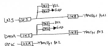
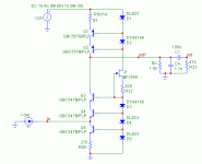
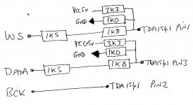
Hi Builder Brad,
Almost, I no longer use a damping resistor for BCK input (buffer > DAC clock input is less than half of an inch).
Both 3K3 and 1K are connected to the DAC chip input, and both 1K5 and 1K8 are connected in series. I placed 1K5 close to the transmitter, and the 1K8 close to the DAC chip input.
1K5 > PCB trace > 1K8 > DAC chip input.
3K3 from DAC chip input to VCC
1K from DAC chip input to GND.
The attenuator was tested up to 48 KHz sample rate.
For higher sample rates, all resistor values need to be lowered.
I read back into this thread to see if I could find more info on the current attenuation scheme for the WS, BCK and DATA streams, and have posted the following sketch just to be sure that I have got it right:
Almost, I no longer use a damping resistor for BCK input (buffer > DAC clock input is less than half of an inch).
Both 3K3 and 1K are connected to the DAC chip input, and both 1K5 and 1K8 are connected in series. I placed 1K5 close to the transmitter, and the 1K8 close to the DAC chip input.
1K5 > PCB trace > 1K8 > DAC chip input.
3K3 from DAC chip input to VCC
1K from DAC chip input to GND.
The attenuator was tested up to 48 KHz sample rate.
For higher sample rates, all resistor values need to be lowered.
-ecdesigns- said:Convert to differential DEM clock:
- Use U1 pin 3 for 352.8 KHz DEM clock
- Remove C19 (470pF).
- Read post #2441 for DEM clock circuit details.
I try my best going thru the info in this thread but I am lost. I am using the CS 8412, 74HC4040 and TDA 1541 as in post #2446. I would need an external power master clock to replace the on board XO. what additional components do I need. A schematic or diagram would help.
There is still room for improvement. You could add I2S attenuators on DATA / WS. The power supply (decoupling) could be improved, 10uF decoupling caps will hardly have any effect, you might increase them to 220 ... 1000uF.
The master clock isn't synchronized with the source clock, either synchronize the source (slave clock operation), or synchronize the master clock (requires VCXO).
I would also increase MSB active divider decoupling capacitor value (U5 pin 13 and pin 18) to 1uF. The OP-amp circuit could be replaced by the circuit published by Rudolf Broertjes.
The decouple cap has been increased to 470uF ELNA SILMIC II.
Yes I would use the 1uF but it will be WIMA MKS 1uF for the MSB. is this ok.
"Charge-transfered" poweramp.
Hi -ECdesigns-
I built what might be the first "charge-transfer" powered amplifier (!?) based in your invention.
A Zero Component Amp (ZCA), single ended class A Mosfet amp, low power to feed my fullrange horns:
http://diyaudioprojects.com/Solid/ZCA/ZCA.htm
Mine is not stock (it never is, he, he) but has a PowerReg, plus the mentioned "charge-transfer" circuit.
Here are some picks:
http://picasaweb.google.com/lh/photo/DBPGMEHS_kM2f_Pev5oCZg?feat=directlink
http://picasaweb.google.com/lh/photo/8DI-hfrJQ2OkYHDig9m4XA?feat=directlink
I had to build my own box which was a pain (and I still have to do the other monoblock!) because of the DIY heatsinks.
I had to lower R4 from the original 3R4...
I guess it sounds like your "direct Mosfet output" prototype...
In a word; it works!
Cheers,
M
PS: yeah more OT, as nobody seems to notice that this thread is about John's, and anybody else's, DAC...
-ecdesigns- said:
The master clock isn't synchronized with the source clock, either synchronize the source (slave clock operation), or synchronize the master clock (requires VCXO).
Hi ecdesigns and thanks for sharing with us your great work!
i wanted to ask you something regarding your #2447 posting,since i also ordered myself one ot that dac kits.
please detail a little bit yor statement regarding synchronizing master clock with the source clock
(in this setup CS8412 is configured in slave mode rather than outputing the remote master clock in master mode and i don't have much experience with this layout)
Thankks,your help much appreciated!
I have looked back through this thread to find the most up to date DEM reclock details, and can only find the schematic posted on page 4 of this HUGE thread:
here: http://www.diyaudio.com/forums/showthread.php?postid=918278#post918278
does anyone know if there are more up to date details on the DEM reclocking, or should I try the scheme from page 4
Brad
here: http://www.diyaudio.com/forums/showthread.php?postid=918278#post918278
does anyone know if there are more up to date details on the DEM reclocking, or should I try the scheme from page 4
Brad
Hi luxury54
The source clock (generated by connected digital audio source) is integrated in the SPDIF signal. This means that SPDIF carries both, DATA and timing signals.
The SPDIF receiver (CS8412) needs to extract both DATA and timing signals. This is done using a PLL (Phase Locked Loop) circuit that synchronizes an internal VCO (Voltage Controlled Oscillator) with the incoming SPDIF signal. This way both, the embedded DATA, and a timing signal for the DAC (BCK / MCK) can be extracted.
The SPDIF receiver can run in two modes, it can either provide the timing signals (BCK and WS) for the connected DAC chip (master mode), or receive clean timing signals from an external low jitter clock (slave mode).
Master mode means that the DAC chip basically runs on timing signals derived from a VCO (inside the SPDIF receiver chip) that contains significant jitter. Data sheet for CS8412/14/16 specifies 200ps rms MCK jitter, in practice this value is increased by other factors like power supply ripple, interference picked-up by the loop filter, and source / interlink induced jitter.
Slave mode means that the DAC chip receives timing signals from a low-jitter crystal oscillator. Now timing jitter could be significantly reduced, and source jitter could be blocked / attenuated.
The problem with slave mode is that you now have two separate clocks, one from the CS8412 (source), and the other from the crystal oscillator. These will have almost the same frequency, but don't run in sync, this could result in dropping (leaving-out), or repeating a sample (sending the same sample value twice).
In practice the lack of synchronization between these two clocks might result in periodic clicks that are clearly audible when playing-back sine wave test signals. The time period between the clicks decreases with increased frequency difference between both clocks.
This is the case with the schematic in post #2447.
The timing signals are derived from the crystal oscillator X1, and are fed to both DAC chip and CS8412 SPDIF receiver that runs in slave-clock mode. There is no provision to synchronize both source and master clock X1.
There are some options to synchronize both clocks:
1) slave the transport, buffer the master clock signal (11.2896 MHz), and feed it back to the source (CD player). This way both DAC and CD player share the same master clock.
2) Use a VCXO / PLL or other circuit to lock / synchronize the master clock (X1) to the source clock.
The required source clock (for frequency comparison) is still available on the MCK pin (slave-clock mode).
I currently use a CS8416 is slave-clock mode, the VCXO (Voltage Controlled Crystal Oscillator) master clock frequency is adjusted using a miniature 12-bit DAC chip that drives the VCXO voltage input using a filter.
Next a small micro-controller is used to measure both source and VCXO master clock with high precision. The micro-controller then calculates the required correction voltage, and sends this value to the 12-bit DAC. This in turn will change the master clock frequency. By doing so, the master clock frequency is synchronized with the source clock. Corrections take place with 2 second intervals
This circuit, plus 4 ultra-high speed clock buffers are placed on a single module, the master clock / tracker module. There is a photograph of this module in post #2412. The final version has additional screening installed on both sides of the PCB.
please detail a little bit yor statement regarding synchronizing master clock with the source clock
The source clock (generated by connected digital audio source) is integrated in the SPDIF signal. This means that SPDIF carries both, DATA and timing signals.
The SPDIF receiver (CS8412) needs to extract both DATA and timing signals. This is done using a PLL (Phase Locked Loop) circuit that synchronizes an internal VCO (Voltage Controlled Oscillator) with the incoming SPDIF signal. This way both, the embedded DATA, and a timing signal for the DAC (BCK / MCK) can be extracted.
The SPDIF receiver can run in two modes, it can either provide the timing signals (BCK and WS) for the connected DAC chip (master mode), or receive clean timing signals from an external low jitter clock (slave mode).
Master mode means that the DAC chip basically runs on timing signals derived from a VCO (inside the SPDIF receiver chip) that contains significant jitter. Data sheet for CS8412/14/16 specifies 200ps rms MCK jitter, in practice this value is increased by other factors like power supply ripple, interference picked-up by the loop filter, and source / interlink induced jitter.
Slave mode means that the DAC chip receives timing signals from a low-jitter crystal oscillator. Now timing jitter could be significantly reduced, and source jitter could be blocked / attenuated.
The problem with slave mode is that you now have two separate clocks, one from the CS8412 (source), and the other from the crystal oscillator. These will have almost the same frequency, but don't run in sync, this could result in dropping (leaving-out), or repeating a sample (sending the same sample value twice).
In practice the lack of synchronization between these two clocks might result in periodic clicks that are clearly audible when playing-back sine wave test signals. The time period between the clicks decreases with increased frequency difference between both clocks.
This is the case with the schematic in post #2447.
The timing signals are derived from the crystal oscillator X1, and are fed to both DAC chip and CS8412 SPDIF receiver that runs in slave-clock mode. There is no provision to synchronize both source and master clock X1.
There are some options to synchronize both clocks:
1) slave the transport, buffer the master clock signal (11.2896 MHz), and feed it back to the source (CD player). This way both DAC and CD player share the same master clock.
2) Use a VCXO / PLL or other circuit to lock / synchronize the master clock (X1) to the source clock.
The required source clock (for frequency comparison) is still available on the MCK pin (slave-clock mode).
I currently use a CS8416 is slave-clock mode, the VCXO (Voltage Controlled Crystal Oscillator) master clock frequency is adjusted using a miniature 12-bit DAC chip that drives the VCXO voltage input using a filter.
Next a small micro-controller is used to measure both source and VCXO master clock with high precision. The micro-controller then calculates the required correction voltage, and sends this value to the 12-bit DAC. This in turn will change the master clock frequency. By doing so, the master clock frequency is synchronized with the source clock. Corrections take place with 2 second intervals
This circuit, plus 4 ultra-high speed clock buffers are placed on a single module, the master clock / tracker module. There is a photograph of this module in post #2412. The final version has additional screening installed on both sides of the PCB.
Hi Builder Brad,
The latest DEM clock circuit (used in the DI4T and D1) is the differential DEM clock. I will try to post a schematic diagram soon. The new DEM clock requires a 352.8 KHz non inverted and a 352.8 KHz inverted drive signal. These can be derived from the masterclock using a 74HCT4040 or 74HC163 counter, don't use a separate oscillator for this.
Each connected TDA1541A requires a separate differential attenuator / injector circuit consisting of 2 x 1K2, 1 x 330 Ohms, and 2 x 1nF ceramic caps. The attenuator should be placed as close as possible to pins 17 & 18 of the TDA1541A, SMD components are preferred.
The circuit "manipulates" the built-in DEM clock oscillator, by forcing it to run on an external frequency. This has to be done correctly, otherwise the internal DEM oscillator may start oscillating as well (spurious oscillations).
The DEM clock drives shift-registers inside the TDA1541A. These shift-registers operate electronic switches that are used in the active current dividers. These dividers split an input current into multiple equal output currents. The active dividers use the Dynamic Element Matching technique for achieving close tolerance independent of component / chip aging.
The ripple current introduced by initial component tolerances in the passive dividers that are part of the active dividers, is filtered using simple RC filters. The resistor is integrated in the TDA1541A, the filter capacitor is located outside the TDA1541A (decoupling cap).
The reason for synchronizing the DEM clock is to minimize on-chip crosstalk / inter-modulation, and thus minimizing (on-chip) timing jitter. Other advantage is that by providing accurate crystal-controlled timing intervals between toggling the electronic switches, could result in even higher bit accuracy of the active dividers.
I have looked back through this thread to find the most up to date DEM reclock details, and can only find the schematic posted on page 4 of this HUGE thread:
The latest DEM clock circuit (used in the DI4T and D1) is the differential DEM clock. I will try to post a schematic diagram soon. The new DEM clock requires a 352.8 KHz non inverted and a 352.8 KHz inverted drive signal. These can be derived from the masterclock using a 74HCT4040 or 74HC163 counter, don't use a separate oscillator for this.
Each connected TDA1541A requires a separate differential attenuator / injector circuit consisting of 2 x 1K2, 1 x 330 Ohms, and 2 x 1nF ceramic caps. The attenuator should be placed as close as possible to pins 17 & 18 of the TDA1541A, SMD components are preferred.
The circuit "manipulates" the built-in DEM clock oscillator, by forcing it to run on an external frequency. This has to be done correctly, otherwise the internal DEM oscillator may start oscillating as well (spurious oscillations).
The DEM clock drives shift-registers inside the TDA1541A. These shift-registers operate electronic switches that are used in the active current dividers. These dividers split an input current into multiple equal output currents. The active dividers use the Dynamic Element Matching technique for achieving close tolerance independent of component / chip aging.
The ripple current introduced by initial component tolerances in the passive dividers that are part of the active dividers, is filtered using simple RC filters. The resistor is integrated in the TDA1541A, the filter capacitor is located outside the TDA1541A (decoupling cap).
The reason for synchronizing the DEM clock is to minimize on-chip crosstalk / inter-modulation, and thus minimizing (on-chip) timing jitter. Other advantage is that by providing accurate crystal-controlled timing intervals between toggling the electronic switches, could result in even higher bit accuracy of the active dividers.
This circuit, plus 4 ultra-high speed clock buffers are placed on a single module, the master clock / tracker module. There is a photograph of this module in post #2412. The final version has additional screening installed on both sides of the PCB.
Can the finished item in #2412 be hooked up to the schematic as in #2447 [single TDA1541a version, CS8412 in slave mode] . Pls send me a pm if the item is available for sale.
rgds.
John (-ecdesigns-),
Have you tried a transformer-coupled DEM clock drive? I think you mentioned this method earlier. I like this idea, because it would provide true differential, ground-independent driving. I am planning to try a small 455 kHz IF transformer (tuning capacitor removed to make it wideband), like that used in old MW transistor radios.
Laszlo
-ecdesigns- said:There are some options to synchronize both clocks:
1) slave the transport, buffer the master clock signal (11.2896 MHz), and feed it back to the source (CD player). This way both DAC and CD player share the same master clock.
Dear John (ecdesigns),
Thank you very much for your detailed explanation on these facts!
Thanks to you I did understand now very well the things we are dealing with here...
my only question would be regarding the first option that you explained here to synchronize both clocks - and that is:
what if my transport runs on 16.934 Mhz Crystall ??
what can it be done in this case?
because on that schematic we have only one 11.289 mhz oscilator that drives both TDA chip and CS8412 in slave mode.
is there some optimal thing that can be done to synchronize this transport running on 16.934 mhz clock?
Im very curious about your answer on this.
Thank you and Best regards!
- Home
- Source & Line
- Digital Line Level
- Building the ultimate NOS DAC using TDA1541A