Hi maxlorenz,
The DI DACs use Philips stereo DAC chips, so both L and R channel samples appear virtually simultaneous at the DAC outputs. Philips TDA1543 datasheet indicates < 0.2us difference. The latch signal is generated on-chip on the first positive going edge of BCK after WS has gone low.
The DI system drives the stereo chips with time delays, so there will be a time delay between subsequent samples, but not between L/R channels.
As far as I understand, the analog outputs L/R are simultaneous as long as there is info to output...a mono recording or a test signal should show this.
The DI DACs use Philips stereo DAC chips, so both L and R channel samples appear virtually simultaneous at the DAC outputs. Philips TDA1543 datasheet indicates < 0.2us difference. The latch signal is generated on-chip on the first positive going edge of BCK after WS has gone low.
The DI system drives the stereo chips with time delays, so there will be a time delay between subsequent samples, but not between L/R channels.
Hi peufeu,
I use low Rdson FETs in order to maximize passive series resistor value. FET Rdson has different properties when compared with a pure passive resistor with the same value. The passive series resistor is used to accurately control the sustained transfer current.
The peak current flowing through the MOSFET gate during switch-on is already reduced using 1.11 M Ohm gate series resistor. This resistor forms a RC filter with R = 1.11 M Ohm, and C = 1.1nF (2SJ380). It will prevent peak charge transfer current during switching-on of the MOSFET.
Just a question about the charge transfer PSU : you say a low rdson mosfet is good, then you put a 2R resistor in series. Since mosfets with a higher rdson have lower capacitance (usually) would it make a difference to use (say) something with 0.5 ohm rdson but a low capacitance ?
I use low Rdson FETs in order to maximize passive series resistor value. FET Rdson has different properties when compared with a pure passive resistor with the same value. The passive series resistor is used to accurately control the sustained transfer current.
Also in simulations I see that a resistor between source and grid (acting as a voltage divider) can soften the current pulse going through the mosfet.
The peak current flowing through the MOSFET gate during switch-on is already reduced using 1.11 M Ohm gate series resistor. This resistor forms a RC filter with R = 1.11 M Ohm, and C = 1.1nF (2SJ380). It will prevent peak charge transfer current during switching-on of the MOSFET.
-ecdesigns- said:I use low Rdson FETs in order to maximize passive series resistor value. FET Rdson has different properties when compared with a pure passive resistor with the same value. The passive series resistor is used to accurately control the sustained transfer current.
The peak current flowing through the MOSFET gate during switch-on is already reduced using 1.11 M Ohm gate series resistor. This resistor forms a RC filter with R = 1.11 M Ohm, and C = 1.1nF (2SJ380). It will prevent peak charge transfer current during switching-on of the MOSFET.
OK, this makes sense.
I'm looking for easier to find transistors... PyroVeso posted the N-channel FET equivalents : 2SK2232 IRL540N IRL530N
For the P-channel FET, Toshiba docs point to 2SJ412, which is stocked at DigiKey, there is also IRL5602 (but 20V max, so only suitable for the cap-multiplier). I like TO220 packages better, though.
maxlorenz said:Hi Art,
Good to hear that.
I also will mod my CD PRO power supply.I have plenty of V to waste.
Ordered some high V, high power Mosfets and shottkys to mod amplifier power supplies.
No matter how high the PSRR is, one can always do better...that is why John is my hero
Hello Maxlorenz
A friend of mine and me would like to build 2 NelsonPass style F5 amps. He will be responsible for the boards, I for the parts. Even if I have bought all the parts for 4 charge transfer PS for another project, it has dawned on me only when I have read your post, that it could be possible to build such a supply for a power amp as well.
Probably it is possible to use less capacity because of the multiplier.
So I would be interested to know, which different parts you use, especially the Mosfets, which should have very low Rds. The F5 is driven in class a, idle current is 1.1 A/channel.
I thank you for your help
Andre
Hi Rolls,
I hate to search for the parts so I picked up what my present source (Futurlec) had and seemed OK to me>
IRF5210 *P channel.
IRF630 *N channel.
2SK1058 *N channel, good for power amp also
Vishay, MBR20100CTKPBF Diode, barrier, Schottky, dual, CC, 20A, 100V, TO2204 at RS online.
I hope I did it right...
Well, time for me to go to the lake for a week (no internet)
Good luck in your projects.
M
I hate to search for the parts so I picked up what my present source (Futurlec) had and seemed OK to me>
IRF5210 *P channel.
IRF630 *N channel.
2SK1058 *N channel, good for power amp also
Vishay, MBR20100CTKPBF Diode, barrier, Schottky, dual, CC, 20A, 100V, TO2204 at RS online.
I hope I did it right...
Well, time for me to go to the lake for a week
(no internet)Good luck in your projects.
M
maxlorenz said:Hi Rolls,
I hate to search for the parts so I picked up what my present source (Futurlec) had and seemed OK to me>
IRF5210 *P channel.
IRF630 *N channel.
2SK1058 *N channel, good for power amp also
Vishay, MBR20100CTKPBF Diode, barrier, Schottky, dual, CC, 20A, 100V, TO2204 at RS online.
I hope I did it right...
Well, time for me to go to the lake for a week
Good luck in your projects.
M
Thank you, have a nice week.
Andre
Question about charge transfer PS
John,
I am planning on upgrading the power supplies on my DIY TDA1541 DAC and wondered if I should just add the +/-5v and -15v charge transfer stages before the simple LM317 voltage regulators that I use in my DAC, or would I benefit from adding more sophisticated superegulataion after the charge transfer circuit.
regards
Brad
Linear AN101
http://www.linear.com/pc/downloadDocument.do?navId=H0,C1,C1154,C1002,C1243,P1981,D11877
Standard regulators have very low rejection at high frequencies, ie. the noise gets straight through. Hence putting a good PSU before them (including the capacitance multiplier which removes the HF noise) can be expected to provide good effect. You can always try other regs later though...
Hi Builder Brad,
Use the charge transfer circuit and the capacitance multiplier in the power supply. Then route this voltage to a local voltage regulator, placed as close to the TDA1541A as possible. LM317 produces significantly more noise than plain 78xx or 79xx voltage regulators (check data sheets). Noise increases with output voltage, and the regulators will produce specified noise even when connected to a zero noise power supply.
However, it's easy to significantly reduce this noise level by connecting 220 ... 1000uF capacitor between the regulator output pin and GND.
I am planning on upgrading the power supplies on my DIY TDA1541 DAC and wondered if I should just add the +/-5v and -15v charge transfer stages before the simple LM317 voltage regulators that I use in my DAC, or would I benefit from adding more sophisticated superegulataion after the charge transfer circuit.
Use the charge transfer circuit and the capacitance multiplier in the power supply. Then route this voltage to a local voltage regulator, placed as close to the TDA1541A as possible. LM317 produces significantly more noise than plain 78xx or 79xx voltage regulators (check data sheets). Noise increases with output voltage, and the regulators will produce specified noise even when connected to a zero noise power supply.
However, it's easy to significantly reduce this noise level by connecting 220 ... 1000uF capacitor between the regulator output pin and GND.
Question about charge transfer PS
thank-you John, I have a number of superregulator pcbs from Peranders (P_A) web site - JSR03 details here:
http://sjostromaudio.com/joomla/index.php?option=com_content&task=view&id=57&Itemid=27
I have used several of Peranders designs with very good results, so would I benefit from using these super regs after your charge transfer circuit - or even a simple shunt stye reg, rather than the LM series ICs?
Brad
Use the charge transfer circuit and the capacitance multiplier in the power supply. Then route this voltage to a local voltage regulator, placed as close to the TDA1541A as possible. LM317 produces significantly more noise than plain 78xx or 79xx voltage regulators (check data sheets). Noise increases with output voltage, and the regulators will produce specified noise even when connected to a zero noise power supply.
thank-you John, I have a number of superregulator pcbs from Peranders (P_A) web site - JSR03 details here:
http://sjostromaudio.com/joomla/index.php?option=com_content&task=view&id=57&Itemid=27
I have used several of Peranders designs with very good results, so would I benefit from using these super regs after your charge transfer circuit - or even a simple shunt stye reg, rather than the LM series ICs?
Brad
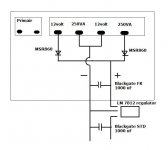
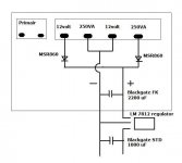
BMW850 said:Sorry the Blackgate 1000 uF FK is a Blackgate 2200 uF FK.
Rudy
Your connection is ok but I think your labelling might be confusing.
Hi BMW850,
I would add some small resistors (0.5 ... 1 Ohm) in series with the diodes to limit peak currents during charging, but you have to check if this doesn't cause too much voltage drop.
Power supply requirements for the master clock are highly critical, these power supplies need to be very clean. I use additional LC filters to achieve this.
I did it on this way for my DDDAC1543 MK2 FULL-24 Kit, 500VA 2x12volt
Is this the right way to make a good supply?
I would add some small resistors (0.5 ... 1 Ohm) in series with the diodes to limit peak currents during charging, but you have to check if this doesn't cause too much voltage drop.
Power supply requirements for the master clock are highly critical, these power supplies need to be very clean. I use additional LC filters to achieve this.
Hi Builder Brad,
These regulators from Peranders should be fine, but they will probably pass HF noise through the series regulator transistors combined parasitic capacitance. This would require some correction (chokes / ferrite beads).
.I have used several of Peranders designs with very good results, so would I benefit from using these super regs after your charge transfer circuit - or even a simple shunt stye reg, rather than the LM series ICs?
These regulators from Peranders should be fine, but they will probably pass HF noise through the series regulator transistors combined parasitic capacitance. This would require some correction (chokes / ferrite beads).
best configuration
Hi ECdesigns. I've readed some articles, and I find them very interesting, because since a long time ago I am designing a 1541 based dac. So I have a question, in your opinnion, what is the best configuration for this TDA1541-A dac? Do you have a schematic? I've modified some players from Marantz, Philips, micromega and so on, and every time I hear this DAC sound, i like it more.
Regards, galeb
- Home
- Source & Line
- Digital Line Level
- Building the ultimate NOS DAC using TDA1541A