This looks like the perfect project to re-juvinate my Buffalo IIIse. I'm running dual mono into the tube-i-zator tube output stage but I've never been 100% satisfied as I think the impedance matching between the current output dac and the valves is well off and this looks like it may pay worthwhile dividends over/different to the Legato 3.1 which I also have. So...I'm going to give this a go! bigpandhahk has been kind enough to sell me his spare kit but I have a few questions...for starters:
1) I have a couple of toroids kicking about from an old project. They're rated 2 x 40-0-40vac output at 80VA per transformer. They are centre-tapped, is that OK? I noticed that on another of Owen's projects this configuration wasn't suited so I thought I'd check. I also understand that the recommended power rating is 50VA but it's not a huge problem is it?
2) I would like to try dual mono by bridging the outputs of each of the BIIIse's and using a single NTD1 board. I think the excess heat/space/FET matching requirements for dual NTD1's is probably overkill ;-) With this in mind, this has been discussed before and I understand that I need to halve the gain and IV resistors, which I am assuming are R13,14, 16, 17, 25, 26, 28, 29?
3) Also regarding dual mono, in this post there was mention of lowering the rails (http://www.diyaudio.com/forums/digi...assic-pass-labs-d1-ess-dac-8.html#post2407111). Is there any guidance as to what to lower them to?
Thanks very much for a fascinating read so far and I am looking forward to posting some pics and progress reports when everything arrives!
Cheers,
Crom
Hi Crom,
Sorry for the delay... I've been busy packing up board orders and haven't been replying on threads as often.
To address your questions:
This is fine for the NTD1 as it uses complimentary (+ and -) regulators, so the GND is common on the whole channel. Only the floating supplies on the new PSU require complete isolation of the AC inputs.
That is correct. You need to roughly halve each resistance value to get half the gain. This will double the current draw given the same rail voltage, which in turn doubles the power dissipation to nearly 100W. If I were to build such a thing, I would reduce the rail voltage down to +/- 32V and use two PSU V2 supplies instead of the on-board supply. This will make power dissipation a little more manageable, dramatically improve the supply performance and noise, and will also improve overall performance thanks to the higher idle current. I would consider the above arrangement as the "ultimate" NTD1. I can provide the NTD1 boards with the supply cut off for exactly this application.
See above")
I will post a modified schematic later this evening to show exactly what resistance value to use, and what the overall power dissipation would be.
Cheers,
Owen
Sorry for the delay... I've been busy packing up board orders and haven't been replying on threads as often.
To address your questions:
1) I have a couple of toroids kicking about from an old project. They're rated 2 x 40-0-40vac output at 80VA per transformer. They are centre-tapped, is that OK? I noticed that on another of Owen's projects this configuration wasn't suited so I thought I'd check. I also understand that the recommended power rating is 50VA but it's not a huge problem is it?
This is fine for the NTD1 as it uses complimentary (+ and -) regulators, so the GND is common on the whole channel. Only the floating supplies on the new PSU require complete isolation of the AC inputs.
2) I would like to try dual mono by bridging the outputs of each of the BIIIse's and using a single NTD1 board. I think the excess heat/space/FET matching requirements for dual NTD1's is probably overkill ;-) With this in mind, this has been discussed before and I understand that I need to halve the gain and IV resistors, which I am assuming are R13,14, 16, 17, 25, 26, 28, 29?
That is correct. You need to roughly halve each resistance value to get half the gain. This will double the current draw given the same rail voltage, which in turn doubles the power dissipation to nearly 100W. If I were to build such a thing, I would reduce the rail voltage down to +/- 32V and use two PSU V2 supplies instead of the on-board supply. This will make power dissipation a little more manageable, dramatically improve the supply performance and noise, and will also improve overall performance thanks to the higher idle current. I would consider the above arrangement as the "ultimate" NTD1. I can provide the NTD1 boards with the supply cut off for exactly this application.
3) Also regarding dual mono, in this post there was mention of lowering the rails (http://www.diyaudio.com/forums/digit...ml#post2407111). Is there any guidance as to what to lower them to?
See above
I will post a modified schematic later this evening to show exactly what resistance value to use, and what the overall power dissipation would be.
Cheers,
Owen
Thanks for coming back to me Owen. This sounds very interesting...
OK, this sounds good. Is the 'new PSU' that you mention above the PSU V2 mentioned below? If so, then I assume from your comment that I'd need 2 independent secondaries which are not centre-tapped?This is fine for the NTD1 as it uses complimentary (+ and -) regulators, so the GND is common on the whole channel. Only the floating supplies on the new PSU require complete isolation of the AC inputs.
I'm liking the sound of this ;-) Where can I find information about the new PSU?That is correct. You need to roughly halve each resistance value to get half the gain. This will double the current draw given the same rail voltage, which in turn doubles the power dissipation to nearly 100W. If I were to build such a thing, I would reduce the rail voltage down to +/- 32V and use two PSU V2 supplies instead of the on-board supply. This will make power dissipation a little more manageable, dramatically improve the supply performance and noise, and will also improve overall performance thanks to the higher idle current. I would consider the above arrangement as the "ultimate" NTD1. I can provide the NTD1 boards with the supply cut off for exactly this application.
Great, thank you. I'll take a look when you post the schematic and get back to you.I will post a modified schematic later this evening to show exactly what resistance value to use, and what the overall power dissipation would be.
Hi Crom,
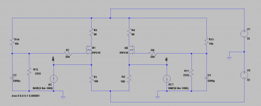
Attached is the schematic for the lower gain version using 32V supplies. This setup gives exactly 2VRMS out at 0dBFS with a mono ES9018 DAC. It also draws 180mA for each leg, giving a total dissipation of 46W which is pretty much what the original version does.
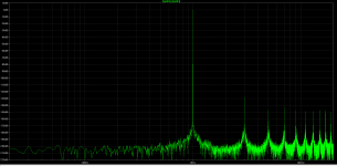
Also attached is the simulated distortion plot at -6dBFS. Since it's a perfect simulation of a differential circuit, the even harmonics are non-existent, but in the real world small imbalances between each leg will result in some even order distortion. Based on measurements, the even order products are about 10dB lower than the odd order harmonics, so you can use your imagination to fill in the blanks.
In the end you get a better power supply, lower noise, lower distortion and you don't give up anything in terms of dissipation.
As for the supply, I was referring to these:
http://www.diyaudio.com/forums/vend...-here-bal-bal-se-se-lpuhp-15.html#post3699950
Cheers,
Owen
Attached is the schematic for the lower gain version using 32V supplies. This setup gives exactly 2VRMS out at 0dBFS with a mono ES9018 DAC. It also draws 180mA for each leg, giving a total dissipation of 46W which is pretty much what the original version does.
Also attached is the simulated distortion plot at -6dBFS. Since it's a perfect simulation of a differential circuit, the even harmonics are non-existent, but in the real world small imbalances between each leg will result in some even order distortion. Based on measurements, the even order products are about 10dB lower than the odd order harmonics, so you can use your imagination to fill in the blanks.
In the end you get a better power supply, lower noise, lower distortion and you don't give up anything in terms of dissipation.
As for the supply, I was referring to these:
http://www.diyaudio.com/forums/vend...-here-bal-bal-se-se-lpuhp-15.html#post3699950
Cheers,
Owen
Attachments
Hi Owen,
Thanks for the Schematic. The closest I can get to for R3& R4 is 100R (Caddock MP930). Also for R1&2 the closest would be 200R. Does this level of accuracy matter?
I'm also having a challenge matching the components from the main schematic and it also looks like some values of other components has changed between the original schematic and this one. Is the below is correct?
Using the schematic here as a reference to compare with the above schematic: http://www.diyaudio.com/forums/atta...-classic-pass-labs-d1-ess-dac-opdac-final.pdf
New schematic opdac-final.pdf schematic
R13,14 10kR R12,30 30k9R
R11,12 2k3R VR7,9 5kR
C3,4 2200uF C35,C45 10uF
Do I follow the new schematic for these other component values or the original?
If I can only get 100/200R values is it possible to re-run the simulation with those values and will this give different component values for the other components?
Sorry, probably stupid questions but I'm still learning ;-)
The closest I can get to for R3& R4 is 100R (Caddock MP930). Also for R1&2 the closest would be 200R. Does this level of accuracy matter?
This problem has been solved. texas components will create custom values, which is great. This means that I can get the exact values that you specify for the gain and IV but need to understand whether I need to source difference values for the components above as well, or, stick to the original bom.
Hi Crom,
The circuit I posted was only for the voltages and the resistor values of the 4 gain/current set resistors.
The rest of the changes are only for simulation purposes, so you should follow the main schematic.
As for the resistor values themselves, it would be best to have them custom made if possible, but using a 100 and 200 resistor wouldn't be too far off. It just means less current and a little more gain, neither of which are good things...
As an alternative to the custom parts, you can order the 100 and 200 ohm resistors, and just parallel a 1206 thin film SMD part between their pins that would give you the exact value you're looking for.
Cheers,
Owen
Thanks Owen, I am now off and running with my build. I didn't want to clog up this thread so I'm posting to here:
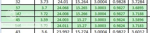
I have managed to get hold of one of your original matched FET quads (kindly from bigpandhahk). It's group 10, see details here:
Is there any particular position within the quad I should be using these in? For example, pairing the nearest numbers in a particular column or balancing the highest value with the lowest...or something like that.
You got a good quad!
I would probably pair them according to transconductance, so 57/142 in one channel, and 45/146 in the other. Overall though, these are such a good match that it probably won't make any difference.
In addition to these parts, matching on the four resistors is also critical, so it's worth paying for 0.1% or 0.01% parts here, or hand matching using the parallel high value resistor technique described above.
The more identical the two legs of each channel are, the better the cancellation of second harmonics will be.
Cheers,
Owen
urp, I didn't give the build url: http://www.diyaudio.com/forums/digi...-fifo-opc-ntd1-salas-sslv-56.html#post3799684
The FETs look good don't they ;-))
That's good advice about pairing on transductance - I shall follow. I think my resistors will be OK...
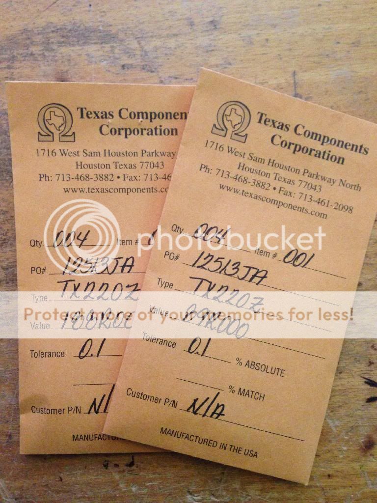
All matching and to spec:

The FETs look good don't they ;-))
That's good advice about pairing on transductance - I shall follow. I think my resistors will be OK...
All matching and to spec:
Hi Crom,
Attached is the schematic for the lower gain version using 32V supplies. This setup gives exactly 2VRMS out at 0dBFS with a mono ES9018 DAC. It also draws 180mA for each leg, giving a total dissipation of 46W which is pretty much what the original version does.
I stupidly missed your 32v supply point when talking about the dual mono config and I've been aiming for 45v. Am I likely to cook something if I hook this up at 45v and should I exchange R6,7,9 & 10 to around 5.1k to be able to tune the voltage to 27-38v?
Thanks,
Crom
Hi Crom,
If you use the above with 45V rails, you'll be dissipating around 90W for a stereo configuration, so the answer to your question really depends on the size of your heatsink and the power rating of those resistors.
I personally wouldn't run it like that.
The whole purpose of the lower voltage rails was to allow you to use the TPS regs on the PSU V2, or even a quad of TPS7A4700 eval regulator boards. If you're putting this much into the dual mono DACs, matched fets and the top notch resistors, it's absolutely worthwhile using a better PSU.
There is a cut line and power supply tie point on each board.
This is essentially the setup I've been working towards, but I won't be going dual mono, and instead will live with 1VRMS output.
In the meantime, if you want to just get it up and running, then adjust the on-board supplies as you mentioned, and work on procuring some alternative supplies while you listen
Cheers,
Owen
Thanks Owen, it's my fault - too hasty - I understand what you're saying and it's good advice. I have separated the psu from the rest of the PSB and am getting up and running by changing the resistor values in the PSU. I now have a steady +/-32v which is great. The plan is certainly to try the PSU V2 upgrade in the near future.
Today I built the I/V circuit and have just checked and then hooked it up. Before I connected anything I reduced the bias trim pots to 0R as I read somewhere in this thread.
When I hooked up the power I got -3.3v across the Source with refg to GND on Q1. Using the trimpot I tweaked until I reached the other end of the resistor but can't get more than 1v. I tried the other half of the left channel (Q3) and managed to get to 1.1v.
Other Q1 voltages:
Source > GND = -3.3
Drain > GND = 16.83
Gate > GND = 4.13
Drain > Source = 16.05 (positive term to Drain)
Q3 voltages:
Source > GND = -3.3
Drain > GND = 18.4
Gate > GND = 4.45
Drain > Source =15.5 (positive term to Drain)
I'm guessing I must have done something wrong but I'm not sure what. Or, should I be biasing to a different voltage for the reduced resistors and dual mono?
Hi Crom,
Did you populate the Zener diodes? I'm not sure what board you have, but the zeners are wrong on the early version and from your description, it sounds like that's the issue.
If possible, return each bias pot to 0R, remove all of the zeners from each leg, and try again. If it all biases up fine, then that was your problem. If not, then there's an issue somewhere else, and I'll need pictures to see what's going on.
To get the zener diodes to work, you need to make a little tee-pee with them, so you'll have toe remove them anyhow. I have been running without them in mine from the start, and have never had a problem.
Cheers,
Owen
Hi Owen,
I did, see here(can't see version number on board but hopefully this well tell you which one it is):
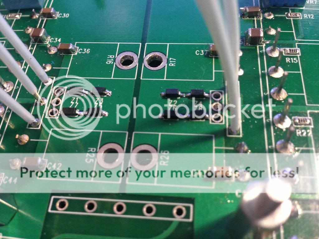
I can't see a version number of the board but I guess it's the same as bigpandhahk had as I got the kit from him. I read about the series / parallel issue but thought these were in series so that was OK. I'm happy to remove them though.
I have also discovered another issue in that I powered up the other side (Q2 and Q4) and I discovered I have drain > GND of 32v for Q2 which seems odd. I've tried re-flowing the joints to the FETS and heatsink-mounted resistors and removing all the caps on that side to check that they're working - I read that bigpandhahk had similar problem and that it was one of the ceramic caps.
I'll post some pics in a bit.
I did, see here(can't see version number on board but hopefully this well tell you which one it is):
I can't see a version number of the board but I guess it's the same as bigpandhahk had as I got the kit from him. I read about the series / parallel issue but thought these were in series so that was OK. I'm happy to remove them though.
I have also discovered another issue in that I powered up the other side (Q2 and Q4) and I discovered I have drain > GND of 32v for Q2 which seems odd. I've tried re-flowing the joints to the FETS and heatsink-mounted resistors and removing all the caps on that side to check that they're working - I read that bigpandhahk had similar problem and that it was one of the ceramic caps.
I'll post some pics in a bit.
Hi Crom,
That's the V2 board, so the zener diodes are fine as long as you are sure you have them populated in the correct orientation as per the board layout.
My next guess would be that the reduced rail voltage means you can no longer get the gate voltage high enough.
What are:
- The value of the resistors running from the V+ rail to the gate
- The value of the bias pots
You may need to reduce the value of the resistors feeding the bias pots with your reduced rail voltage.
Cheers,
Owen
That's the problem...
My fets take about 5V on the gates to get everything where it needs to be.
Do you have some 20k resistors (or something in that ballpark) that you can replace the 30k9 parts with?
Alternatively, something like a 100k in parallel will also work.
Fix that , and you should be up and running. My bad for not checking this when I suggested the lower rail voltages. I didn't realize that resistor was such a high value.
Cheers,
Owen
- Home
- Source & Line
- Digital Line Level
- Build Thread - A New Take on the Classic Pass Labs D1 with an ESS Dac