Thanks for your help Owen - I'm biasing just perfectly!!
Q1: 1.65v
Q3: 1.65v
Q4: 1.65v
I've still got that problem with Q2 though. V strange voltages compared to the other 3:
Q1
Source > GND = 1.65
Drain > GND = 16.43
Gate > GND = 5.08
Drain > Source = 14.9 (positive terminal to Drain)
Q2
Source > GND = 0
Drain > GND = 32
Gate > GND = 1.621
Drain > Source = 32.15 (positive terminal to Drain)
Q3
Source > GND = 1.65
Drain > GND = 16.43
Gate > GND = 4.97
Drain > Source = 14.83(positive terminal to Drain)
Q4
Source > GND = 1.65
Drain > GND = 16.32
Gate > GND = 5.05
Drain > Source = 14.7 (positive terminal to Drain)
any ideas?
Attachments
Hmm... looks like he gate voltage isn't high enough to get the fet to conduct.
Check:
- Voltage between new (old) resistors and pot
- Voltage before gate resistor
- Voltage after gate resistor
- Voltage on negative supply right on the source resistor
Could be a faulty pot, hopefully not a damaged fet. Reflow all the joints and make extra sure the isolation pad is working between the fet and the heatsink.
Cheers,
Owen
Hi Owen,
Slightly unorthodox but I wanted to make sure that I was interpreting what you asked correctly so I did it visually - all voltages relative to ground.
I have to say this is great learning for me - someone in another thread said that you only learn when something goes wrong...very true!
Isolation pad is doing its job correctly.
Attachments
Last edited:
Very nice diagram! Makes troubleshooting much easier ")
It pretty much has to be one of the following:
- The resistor you added at R12 is faulty, or the wrong value.
- The pot is faulty or not correctly adjusted
- C35 is damaged or faulty and is presenting low impedance to GND.
Of the above three, my money would be on the pot. Try pulling it out and measuring the resistance from end to end, and wiper to each end. You might be able to do it in-circuit with everything off, so try that before pulling it.
My next guess would be the cap, but it's less likely.
With only 1.6V on the gate, the fet will not even begin to conduct, hence the 32V on the drain. With no current flowing through the drain resistor, there will be no voltage drop across it.
What doesn't make sense is that you have 0V on the source, when you should be seeing some negative voltage a little higher than the zener voltage. Not sure what's going on there.
You might want to adjust one of the other legs to have 1.6V on the gate, and see if the voltages match for troubleshooting purposes.
So close! You're 75% up and running
Cheers,
Owen
Last edited:
Owen, with your help I think I'm there!!! )))
What it turned out to be was a tiny spec of solder lodged between the ground and the negative input which leads to Q2 - it wasn't even soldered in place...I just brushed it out the way. This was clearly left over by me when I removed the pins I had in there originally and decided to solder wires into the more widely spaced inputs (see pic below). This was after I took the whole thing off the heatsink of course...ha, but it doesn't matter, we're all up and running at the correct voltages and I'm going to put it together and test it with the DAC
Just in case it's of any help to anyone in the future this is the logic (AKA, random guess-work) that I worked through to get there:
Following your instructions:
- I removed R12 and tested: 19.9K.
- With R12 out the way I tested the pot between the GND rail and one of the R12 terminals. The resistance tracked perfectly from 0.2R to 5.1K....looked good to me.
- I found that resistance across C35 and ground = 30R which looked a bit odd (I know the solution is probably obvious to you guys but bear with me)
- I removed C35 and tested - all fine there. When capacitor is removed 30R remains across terminals??
- I then removed C34 to compare to the same place on the L channel. Resistance there is 3.4k
- I then looked at the circuit diagram and realised that the resistance across those capacitors is going to be controlled by the pot and that the left channel was already biased to 1.65v whereas the other wasn't. This explained why one side was 30R and the other much more (big DOH! moment)
- OK, so back on track. I worked through reasons why there would be 0v at source and the most logical was that there was a short to GND somewhere nearby....and sure enough I found one!!
Q1
Source > GND = 1.65
Drain > GND = 16.44
Gate > GND = 5.11
Drain > Source = 14.65 (positive terminal to Drain)
Q2
Source > GND = 1.65
Drain > GND = 16.42
Gate > GND = 5.10
Drain > Source = 14.73 (positive terminal to Drain)
Q3
Source > GND = 1.65
Drain > GND = 16.41
Gate > GND = 4.99
Drain > Source = 14.70 (positive terminal to Drain)
Q4
Source > GND = 1.65
Drain > GND = 16.41
Gate > GND = 5.06
Drain > Source = 14.75 (positive terminal to Drain)
Readings look good
I had to rig up some larger heatsinks onto the power supply as those regs aren't going to last long trying to produce 32v dc from 40vac. Even these larger ones get pretty toasty. I'll dig out some lower voltage transformers before long.
Thanks very much for your help. I'm going to start to connect it into the dac boards now...see what happens!
)))What it turned out to be was a tiny spec of solder lodged between the ground and the negative input which leads to Q2 - it wasn't even soldered in place...I just brushed it out the way. This was clearly left over by me when I removed the pins I had in there originally and decided to solder wires into the more widely spaced inputs (see pic below). This was after I took the whole thing off the heatsink of course...ha, but it doesn't matter, we're all up and running at the correct voltages and I'm going to put it together and test it with the DAC
Just in case it's of any help to anyone in the future this is the logic (AKA, random guess-work) that I worked through to get there:
Following your instructions:
- I removed R12 and tested: 19.9K.
- With R12 out the way I tested the pot between the GND rail and one of the R12 terminals. The resistance tracked perfectly from 0.2R to 5.1K....looked good to me.
- I found that resistance across C35 and ground = 30R which looked a bit odd (I know the solution is probably obvious to you guys but bear with me)
- I removed C35 and tested - all fine there. When capacitor is removed 30R remains across terminals??
- I then removed C34 to compare to the same place on the L channel. Resistance there is 3.4k
- I then looked at the circuit diagram and realised that the resistance across those capacitors is going to be controlled by the pot and that the left channel was already biased to 1.65v whereas the other wasn't. This explained why one side was 30R and the other much more (big DOH! moment)
- OK, so back on track. I worked through reasons why there would be 0v at source and the most logical was that there was a short to GND somewhere nearby....and sure enough I found one!!
Q1
Source > GND = 1.65
Drain > GND = 16.44
Gate > GND = 5.11
Drain > Source = 14.65 (positive terminal to Drain)
Q2
Source > GND = 1.65
Drain > GND = 16.42
Gate > GND = 5.10
Drain > Source = 14.73 (positive terminal to Drain)
Q3
Source > GND = 1.65
Drain > GND = 16.41
Gate > GND = 4.99
Drain > Source = 14.70 (positive terminal to Drain)
Q4
Source > GND = 1.65
Drain > GND = 16.41
Gate > GND = 5.06
Drain > Source = 14.75 (positive terminal to Drain)
Readings look good
I had to rig up some larger heatsinks onto the power supply as those regs aren't going to last long trying to produce 32v dc from 40vac. Even these larger ones get pretty toasty. I'll dig out some lower voltage transformers before long.
Thanks very much for your help. I'm going to start to connect it into the dac boards now...see what happens!
Attachments
Hello,
Just a little word from a newbie that will try to build a ESS9018 with NTD1 I/V stage. I am waiting for PCB order to start. In the meantime, I will try to check this build thread to understand how it works and how to build it correctly.
I hope I won't kill your patience..
Just a little word from a newbie that will try to build a ESS9018 with NTD1 I/V stage. I am waiting for PCB order to start. In the meantime, I will try to check this build thread to understand how it works and how to build it correctly.
I hope I won't kill your patience..
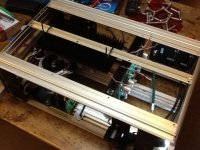
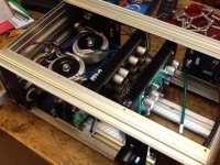
I thought that I would post a few photos of my DAC in its current state. Although not completed by any means, I believe its close.
Since having received quite a few messages concerning my NTD1 build, most of which were related to cooling, I thought it would be a good idea to post current photos of the DAC.
Attachments
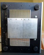
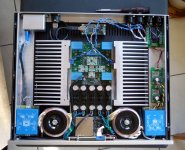
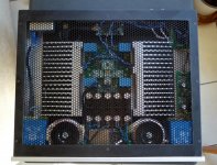
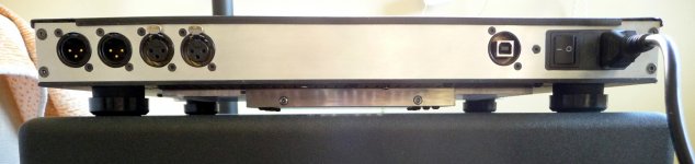
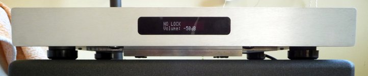
Since having received quite a few messages concerning my NTD1 build, most of which were related to cooling, I thought it would be a good idea to post current photos of the DAC.
Great build!
Funny enough, mine looks a lot like yours! I added an Arduino Uno to control the DAC functions and now I'm thinking of also adding a balanced to unbalanced circuit for unbalanced amplifiers
Buffalo II DAC (ES9018) avec Sortie I/V NTD1 (Pass D1)
Do
I missed the train... But here I am building
And seeking for best layout guys, single SPDIF input for now.
Here are two pictures of the layout I can figure right now, one shows regulators' board laying flat but facing a bit the transformers, 8 cm of wire to the NTD1, the second with regulators' board with best cooling, making a wall between tranformers and NTD1 but adding say 4cm of wire for the DC. Wich is best? Cleaner in my eyes is the second, but more wire between regulators and load is said to be bad... Help!
Attachments
For anyone looking for a board + parts, I've posted my kit for sale on the swap meet board.
I have been trying to track down why I had a small hum from one of my speakers when using the NTD1 and buffalo DAC combo. It was not really an issue when I used my integrated Tube amplifier with volume control. But I just finalised the Sony VFET power amplifier from Nelson Pass and wanted to use this amplifier directly with NTD1. Now it was obvious that I had an issue. I did some trials yesterday evening and found that when I removed the buffalo dac from NTD1 then my speaker was dead silent and no hum could be heard. I then tried to attach the buffalo dac again and the hum was back. I did some more measurements and found that ground connection was missing between buffalo dac and NTD1 on the left channel (channel that have hum) - apparantly I forgot to solder that connection on the buffalo board :-O
But then again I started wondering if I only need to connect + and - output from the buffalo dac to the input of NTD1 or do I need to connect both +, - and G connector from buffalo output to the NTD1 for left and right channel?
Your help is really appreciated - thanks
Søren
But then again I started wondering if I only need to connect + and - output from the buffalo dac to the input of NTD1 or do I need to connect both +, - and G connector from buffalo output to the NTD1 for left and right channel?
Your help is really appreciated - thanks
Søren
I have been trying to track down why I had a small hum from one of my speakers when using the NTD1 and buffalo DAC combo. It was not really an issue when I used my integrated Tube amplifier with volume control. But I just finalised the Sony VFET power amplifier from Nelson Pass and wanted to use this amplifier directly with NTD1. Now it was obvious that I had an issue. I did some trials yesterday evening and found that when I removed the buffalo dac from NTD1 then my speaker was dead silent and no hum could be heard. I then tried to attach the buffalo dac again and the hum was back. I did some more measurements and found that ground connection was missing between buffalo dac and NTD1 on the left channel (channel that have hum) - apparantly I forgot to solder that connection on the buffalo board :-O
But then again I started wondering if I only need to connect + and - output from the buffalo dac to the input of NTD1 or do I need to connect both +, - and G connector from buffalo output to the NTD1 for left and right channel?
Your help is really appreciated - thanks
Søren
I think it would make more sense to connect grounds between the Buffalo's and NTD1's power supplies, and leave the signal output ground out.
Ok, I know I might be the last person to make the ntd1 but here it is anyway
And I just want to share this build.
I was able to purchase a kit (v1?) through a member with all the essential parts. Perhaps he wants to be anonymous but thank you!
Unfortunately opc don't respond to messages or on vendors bazaar. I wanted to buy a v3...and it's still on the list.
Anyway, I have a non working Audionet and my luck is that it has a +-51VDC supply. So out with the amplifier board and in with the cooling fin (Conrad) and the ntd1 board.
I use the 750 and 390 ohm caddocks to get enough voltage to feed my F5 directly.
Setting up to board went like clockwork and it's playing beautifully
I tapped the motor pot outputs from the CPU. So I can use the original remote control.
And I'm using SE output. So only caps on pos output. I did try Lundahl trafo to convert bal-SE and that sounded good as well. But the best was to use a 47k dummy load on the bal- output. I made the sound go from a bit dull and not so airy to shimmering and sparkling.
I want to thank opc and all the time, effort and excellent engineering that was put into this project.
And I'm using SE output. So only caps on pos output. I did try Lundahl trafo to convert bal-SE and that sounded good as well. But the best was to use a 47k dummy load on the bal- output. I made the sound go from a bit dull and not so airy to shimmering and sparkling.
I want to thank opc and all the time, effort and excellent engineering that was put into this project
.- Home
- Source & Line
- Digital Line Level
- Build Thread - A New Take on the Classic Pass Labs D1 with an ESS Dac