ONsemi list MJW0281/0302Giaime said:
Are you sure of the bjt names? I can't find them.
Does 2SA970 have a complementary npn type? Should it be the 2SC2240?
2sa970/c2240 are the complementary pair.
AndrewT said:
ONsemi list MJW0281/0302
Interesting. I wonder if they are enough for my application, instead of MJL3281 (200W Pdiss vs. 150W).
But I fear that SPICE models for Philips transistors (BD139-BD140) are not accurate: in reality they should be not worse than the japanese transistors I'm using now in the simulation, but in SPICE they are far worse. Also BD139-140 is cheaper and far more available...
I think I'll start a PCB design for the amp.
Giaime's schematic
Giaime
The O/P devices you mentioned would probably be quite
satifactory, but why not use the 2SC5200/2SA1943 Toshiba devices ? They are much easier to obtain, and places such as Ampslab, even sell them as 5 matched pairs, at quite a good price.Re the BD139/BD140, I think that you will have great difficulty getting complete data on these devices. Their performance also seems to vary dramatically, depending on who the manufacturer is.
Another excellent choice for driver transistors, is the 2SC5171/2SA1930.These are fabulous driver devices, and also available from Ampslab in packets of 10. I highly recommend these devices for use with an amplifier of the quality you are attempting to achieve. Allan, from Sydney has fitted these in the new Silicon Chip 20W Class A amplifier, with extremely good results. We are also using them in several other designs "Down Under".I know that Jacco thinks very highly of these devices also.
Regards
SandyK
jaycee said:Do not use the BD139/140 SPICE models from Onsemi. They are wrong. Use the ones from Fairchild.
I never managed to learn the procedure to add models in Orcad Capture. Does someone know a link with a good explanation?
Re: Giaime's schematic
Hello Alex,
mmmmmhhh. Sincerely, I don't understand. I'm using mixed NFB method a la Leach, and those capacitors are plainly needed. C6 is there also to block DC from skewing up the output offset, its value is so low because VAS nfb comes in play only when output nfb goes down (thanks to C7). Those values are optimized to give a flat response: though I can't find a suitable 180pF cap, I found that 200pF (100p//100p) is equally good.
If you are asking why I don't use only output NFB, I answer that this way can get away with a smaller Cdom capacitor, without loosing too much phase margin.
Instead, if you're asking why I don't use NFB only from the VAS, well that's because distortion goes up with a factor of three.
I can always revert to a more common output-only NFB method, by removing C6 and C7 from the PCB, maybe using a phase lead network to gain further phase margin.
However what you said interested me: I started the design using Leach style NFB and forgot about it, maybe it can be useful to reiterate stability analysis now that the amp is (almost) in its definitive state. I will post later the results")
Hello Alex,
sandyK said:Giaime
Have you tried simulations without C6 and C7 ?
Most similar designs don't find them necessary,or are they necessary because of the CFP input stage? If this is the reason , it seems a terrible tradeoff for their use.
SandyK
mmmmmhhh. Sincerely, I don't understand. I'm using mixed NFB method a la Leach, and those capacitors are plainly needed. C6 is there also to block DC from skewing up the output offset, its value is so low because VAS nfb comes in play only when output nfb goes down (thanks to C7). Those values are optimized to give a flat response: though I can't find a suitable 180pF cap, I found that 200pF (100p//100p) is equally good.
If you are asking why I don't use only output NFB, I answer that this way can get away with a smaller Cdom capacitor, without loosing too much phase margin.
Instead, if you're asking why I don't use NFB only from the VAS, well that's because distortion goes up with a factor of three.
I can always revert to a more common output-only NFB method, by removing C6 and C7 from the PCB, maybe using a phase lead network to gain further phase margin.
However what you said interested me: I started the design using Leach style NFB and forgot about it, maybe it can be useful to reiterate stability analysis now that the amp is (almost) in its definitive state. I will post later the results
Bah. I guess that from standard, SPICE based stability criteria, it doesn't change too much between different NFB methods (but I think C24 should be nearer 82p than 68p).
But... this NFB method give me more confidence. To have the input stage "isolated" from NFB taken directly from the load, at frequencies where the output stage and the load may show indesiderable interactions... after all, the whole audio band, and the first 3 harmonics of a 20kHz signal, are covered by output NFB. Over 100kHz, VAS NFB takes place: shorter feedback loop, maybe equal to longer one but only in SPICE, in reality I feel more confident this way.
Let's see how it turns out: after all, this is my first amp with those complications
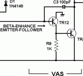
Hi Giaime,
Glad to see you're using a bootstrapping emitter follower Q39 for the VAS voltage gain transistor Q68, and without omitting the overcurrent protection provided by Q69 - R80.
By the way, I think that the collector of Q69 would better be connected to the base of Q68 than to its collector.
I just wonder if adding another emitter follower ahead of Q68, as most published Self schematics, would have any visible effect on distorsion as the CFP input stage can deliver current in a more linear way than a standard twin transistor pair.
There is also a detail, not shown on your shematic, used but remained without comment from Self : a resistor in the collector of Q63, the current source for the input pair. It would lower the dissipation of Q63, I just wonder if it does add some benefits at high frequencies considering the parastitic caps around Q63.
Regards.
Hi,
the input CFP LTP is running with a total tail current of ~3mA.
that's just 0.3mA and ~1.2mA in each of the transistors.
Would the front end perform better if these currents were increased?
I agree completely on the bootstrapped follower after the VAS and with the protection.
I cannot understand why moving the shorting link (q69 collector) from collector to base of q68 makes much difference. is it parasitics again or some other reason, please explain.
I note that C25 is attached to the bottom of R55. Is this better than to the collector of Q40?
What about provision for base stopper resistors for the outputs. Or is this "just in case" of no advantage?
I wonder if Leach's HF NFB that excludes the outputs and drivers increases the HF distortion and other artefacts that I think I can hear?
What about a red or green LED to replace D1&2? less noise? and maybe a // cap as well.
Provision for a series R+C from Q45 collector to -ve rail (another just in case).
How about setting R1 as high as possible and yet still stable with open input connector?
What is the advantage to using 2sa1368 for VAS & CCS?
This schematic looks like a nice mix of "good to have" features.
How did the overall concept come about?
Hello Forr!
Well, I've tried them all around the VAS. Emitter follower before it, cascoding it... with the VAS buffer, there is plain no difference (in SPICE at least). Also I must add that the emitter follower before the VAS worsen the clipping behaviour.
About the overcurrent protection: I don't think the move you suggest is needed. Even this way, a plain short across the output won't kill anything. VAS current drops to nothing, and Q69 saturates, shunting all the driving current for Q39. Even diffamp transistors are protected, they dissipate only a few mW under those faulty conditions.
Maybe it's useful to choose a BD639 for Q69, instead a small BC546: when it saturates it can break the Ic limits for those small To92 bjts.
Nah. As I said, THD is not modified at lower levels, but it shows a bad behaviour at clipping (at least in SPICE).
Good suggestion. Q63 was dissipating only 100mW, and lowering to 45mW with a 8k2 resistor doesn't change much. Small benefits at HF, very hard to distinguish in SPICE. But I like that, and even if it increase the component count, I added it in the schematic.
forr said:Hi Giaime,
Glad to see you're using a bootstrapping emitter follower Q39 for the VAS voltage gain transistor Q68, and without omitting the overcurrent protection provided by Q69 - R80.
By the way, I think that the collector of Q69 would better be connected to the base of Q68 than to its collector.
Well, I've tried them all around the VAS. Emitter follower before it, cascoding it... with the VAS buffer, there is plain no difference (in SPICE at least). Also I must add that the emitter follower before the VAS worsen the clipping behaviour.
About the overcurrent protection: I don't think the move you suggest is needed. Even this way, a plain short across the output won't kill anything. VAS current drops to nothing, and Q69 saturates, shunting all the driving current for Q39. Even diffamp transistors are protected, they dissipate only a few mW under those faulty conditions.
Maybe it's useful to choose a BD639 for Q69, instead a small BC546: when it saturates it can break the Ic limits for those small To92 bjts.
I just wonder if adding another emitter follower ahead of Q68, as most published Self schematics, would have any visible effect on distorsion as the CFP input stage can deliver current in a more linear way than a standard twin transistor pair.
Nah. As I said, THD is not modified at lower levels, but it shows a bad behaviour at clipping (at least in SPICE).
There is also a detail, not shown on your shematic, used but remained without comment from Self : a resistor in the collector of Q63, the current source for the input pair. It would lower the dissipation of Q63, I just wonder if it does add some benefits at high frequencies considering the parastitic caps around Q63.
Regards.
Good suggestion. Q63 was dissipating only 100mW, and lowering to 45mW with a 8k2 resistor doesn't change much. Small benefits at HF, very hard to distinguish in SPICE. But I like that, and even if it increase the component count, I added it in the schematic.
Attachments
Giaime's schematic
Giaime
Forr is correct about the missing collector resistor for Q63.
Normal practice is to drop about half the voltage across the transistor, and about half across the series resistor. This gives better thermal tracking due to reduced temperature rise in Q63.
Regarding my previous comments, a CFP input pair as well as a CFP O/P pair would be a tricky beast to tame at the best of times, without letting the smoke out. Why complicate matters by using techniques from 2 different designers, in what is basically a "blameless" design, but with CFP input ?
BTW, in the other thread you asked about onboard filter capacitor values. 470uF /100nF should be optimum, provided that you are using 24,000-30,000uF per rail with a centrally located PSU PCB using short leads. Tinned braid from heavy duty coax cable, encased in heatshrink, is excellent in this application.
SandyK
Re: Giaime's schematic
Hello friends,
You're perfectly right. This value of tail current is the one that gives lowest THD, at least in SPICE. Changing it is a matter of changing 2 resistors, so it can be tweaked on the real prototype.
No difference in SPICE. Do you think it can be better the way you suggest?
What value you suggest? I see 4.7ohm typical. I've seen that with them, THD and stability gets worse.
I don't know, never tried it. But crossing over at 80kHz... it's a bit much to hear "artefacts", given a good linear output stage that could also be left completely out of global NFB, if only I didn't like 0.00001% THD figures and the like
Interesting. Do you think it's better? I never tried it in an amp, but in a preamp I'm using a LED that way. If you think noise and temperature coefficient would be better, I'll do it, also because it looks cooler
I think I've seen this, but R+C from Q46 collector to -ve rail. The purpose is balancing diffamp currents: how to calculate R and C?
I've seen values of up 1Mohm, I guess it could be done. Is there an advantage, since it's paralleled with 22k?
2SC3421/2SA1358 are good driver transistor. Since BD139/BD140 has a bad model in Orcad Capture, I dismissed those ones in favour of japanese transistors. But Toshibas are harder to find than Philips BDxxx, at least here, and I've been guaranteed that in reality BDxxx are good bjts, so I'll use those in the final design.
I'm glad you think this, and I'm glad you ask. Well, it started with "the basic amplifier" by D. Self (fig 1a in this link). I made it work (it doesn't in the original form, at least in SPICE), then I wanted to try it with Leach style NFB: after this, I started tweaking and tweaking, with an eye on D. Self's book and the other eye to other popular amplifier designs (such as ESPs, GEM, DestroyerX ones, AKSA, and others), incorporating useful features.
Thanks Alex, I just done this, the way you suggest: dropping 20V on the resistor and 20V on the transistor.
You're right. Perfectly right. In fact, I think I will move this way:
- do a PCB that allows all methods of compensation;
- build it up and test the output CFP without including it in global feedback;
- then if it's stable, I'll try global feedback taken only from output;
- then if it sounds better, I'll try Leach style.
So the schematic reflects the "how I want it to be" amplifier, not the "how I managed to make it stable" one
Sorry for writing in another topic, I though it was more pertinent there because it was a question on Carlos' amp PCB. I saw he's using big capacitors, so I asked why, because as I view it, there should be no need of them, once you take care of HF bypassing.
And guess what? While I was waiting for your reply, I just find out that a good combination would be exactly 470uF 63V and 100nF film...
Hello friends,
AndrewT said:Hi,
the input CFP LTP is running with a total tail current of ~3mA.
that's just 0.3mA and ~1.2mA in each of the transistors.
Would the front end perform better if these currents were increased?
You're perfectly right. This value of tail current is the one that gives lowest THD, at least in SPICE. Changing it is a matter of changing 2 resistors, so it can be tweaked on the real prototype.
I note that C25 is attached to the bottom of R55. Is this better than to the collector of Q40?
No difference in SPICE. Do you think it can be better the way you suggest?
What about provision for base stopper resistors for the outputs. Or is this "just in case" of no advantage?
What value you suggest? I see 4.7ohm typical. I've seen that with them, THD and stability gets worse.
I wonder if Leach's HF NFB that excludes the outputs and drivers increases the HF distortion and other artefacts that I think I can hear?
I don't know, never tried it. But crossing over at 80kHz... it's a bit much to hear "artefacts", given a good linear output stage that could also be left completely out of global NFB, if only I didn't like 0.00001% THD figures and the like
What about a red or green LED to replace D1&2? less noise? and maybe a // cap as well.
Interesting. Do you think it's better? I never tried it in an amp, but in a preamp I'm using a LED that way. If you think noise and temperature coefficient would be better, I'll do it, also because it looks cooler
Provision for a series R+C from Q45 collector to -ve rail (another just in case).
I think I've seen this, but R+C from Q46 collector to -ve rail. The purpose is balancing diffamp currents: how to calculate R and C?
How about setting R1 as high as possible and yet still stable with open input connector?
I've seen values of up 1Mohm, I guess it could be done. Is there an advantage, since it's paralleled with 22k?
What is the advantage to using 2sa1368 for VAS & CCS?
2SC3421/2SA1358 are good driver transistor. Since BD139/BD140 has a bad model in Orcad Capture, I dismissed those ones in favour of japanese transistors. But Toshibas are harder to find than Philips BDxxx, at least here, and I've been guaranteed that in reality BDxxx are good bjts, so I'll use those in the final design.
This schematic looks like a nice mix of "good to have" features.
How did the overall concept come about?
I'm glad you think this, and I'm glad you ask. Well, it started with "the basic amplifier" by D. Self (fig 1a in this link). I made it work (it doesn't in the original form, at least in SPICE), then I wanted to try it with Leach style NFB: after this, I started tweaking and tweaking, with an eye on D. Self's book and the other eye to other popular amplifier designs (such as ESPs, GEM, DestroyerX ones, AKSA, and others), incorporating useful features.
sandyK said:Giaime
Forr is correct about the missing collector resistor for Q63.
Normal practice is to drop about half the voltage across the transistor, and about half across the series resistor. This gives better thermal tracking due to reduced temperature rise in Q63.
Thanks Alex, I just done this, the way you suggest: dropping 20V on the resistor and 20V on the transistor.
Regarding my previous comments, a CFP input pair as well as a CFP O/P pair would be a tricky beast to tame at the best of times, without letting the smoke out. Why complicate matters by using techniques from 2 different designers, in what is basically a "blameless" design, but with CFP input ?
You're right. Perfectly right. In fact, I think I will move this way:
- do a PCB that allows all methods of compensation;
- build it up and test the output CFP without including it in global feedback;
- then if it's stable, I'll try global feedback taken only from output;
- then if it sounds better, I'll try Leach style.
So the schematic reflects the "how I want it to be" amplifier, not the "how I managed to make it stable" one
BTW, in the other thread you asked about onboard filter capacitor values. 470uF /100nF should be optimum, provided that you are using 24,000-30,000uF per rail with a centrally located PSU PCB using short leads. Tinned braid from heavy duty coax cable, encased in heatshrink, is excellent in this application.
SandyK
Sorry for writing in another topic, I though it was more pertinent there because it was a question on Carlos' amp PCB. I saw he's using big capacitors, so I asked why, because as I view it, there should be no need of them, once you take care of HF bypassing.
And guess what? While I was waiting for your reply, I just find out that a good combination would be exactly 470uF 63V and 100nF film...
Hi Giaime,
---About the overcurrent protection: I don't think the move you suggest is needed. Even this way, a plain short across the output won't kill anything. VAS current drops to nothing, and Q69 saturates, shunting all the driving current for Q39. Even diffamp transistors are protected, they dissipate only a few mW under those faulty conditions.---
Maybe I'm wrong : I think the move I suggested would be better for recovery overload.
Concerning C25, the blameless amp uses an electrolytic of high value.
Another question : is the connection of Cdom C24 to the emitter of e-follower Q39 would affect the overall stability ?
Of course, this somewhat reminds us the Cherry scheme (Cdom englobing the output stage).
If it is possible to go through this half-way, not to say third way, Cherry's implementation, the output node of the Vas stage would then be at an even lower impedance at HF than the standard blameless circuit.
Regards
Hello Forr!
Boh? Maybe I'll try on the prototype. In SPICE, no difference.
Interesting: I cannot see the benefits of increasing the capacitance much. Maybe someone more experienced can explain: in fact I've always seen 22uF or so there.
Very very good point, thank you In fact looping the VAS buffer in Cdom nfb gives sligtly better results.
.forr said:Maybe I'm wrong : I think the move I suggested would be better for recovery overload.
Boh? Maybe I'll try on the prototype. In SPICE, no difference.
Concerning C25, the blameless amp uses an electrolytic of high value.
Interesting: I cannot see the benefits of increasing the capacitance much. Maybe someone more experienced can explain: in fact I've always seen 22uF or so there.
Another question : is the connection of Cdom C24 to the emitter of e-follower Q39 would affect the overall stability ?
Of course, this somewhat reminds us the Cherry scheme (Cdom englobing the output stage).
If it is possible to go through this half-way, not to say third way, Cherry's implementation, the output node of the Vas stage would then be at an even lower impedance at HF than the standard blameless circuit.
Regards
Very very good point, thank you
In fact looping the VAS buffer in Cdom nfb gives sligtly better results.Re: Re: Giaime's schematic
Another I noticed after my last post.
R80 is set very low.
My thoughts are that the CCS allows the VAS to pass 4mA quiescent amd then AC drive varies this up to a maximum of +-4mA leaving a range of 0mA to 8mA.
If the signal were asymmetrical then -4+6mA might just become feasible. this increases the VAS current range to 0mA to 10mA.
Now consider the protecion transistor.
We normally accept that the Vbe will be between 600mV and 650mV in normal operation. But when you look at the Vbe graphs most transistors start to conduct at about 450mV to 500mV.
Keeping that last bit in mind let's think about good protection and what we expect it to do.
It should be completely inaudible for all valid audio signals.
It should also be inaudible for all valid speaker loads that are within the drive specification.
Finally, it should be inaudible for all combinations of the two previous operating conditions.
If you accept those inaudibility conditions, then my next test is that the protection should limit as early as possible without contravening inaudibility.
If the protection transistor is just starting to conduct @ 450mVbe, then that could be the trigger point for audibility.
The voltage across r80 should generate the minimum Vbe to just start conduction.
Taking that 10mA maximum from earlier and applying it to 470mV the resistor should be about 47r. This is about one third of the CCS resistor.
I use that 3times as my ratio for CCS current in the quiescent VAS to trigger set point.
I would use 150r and 51r not 15r which allows too high a current for no audibility gain.
What do you think?
So Spice forced you into low currents. Try higher gain in the first stage to reduce base current (=input offset current)Giaime said:This value of tail current is the one that gives lowest THD, at least in SPICE.
I was genuinely asking, but intuition tells me that the VAS is driving the CCS voltage. The more direct that AC drive the better. That leads me towards moving the cap to the CCS collector.Giaime said:No difference in SPICE. Do you think it can be better the way you suggest?
1r0 to 2r2, yes a small increase in distortion because the source impedance is raised. I don't understand why it should be less stable with base stoppers in place.Giaime said:What value you suggest? I see 4.7ohm typical. I've seen that with them, THD and stability gets worse.
no. HF compensation is primary purpose.Giaime said:
I think I've seen this, but R+C from Q46 collector to -ve rail. The purpose is balancing diffamp currents: how to calculate R and C?
Another I noticed after my last post.
R80 is set very low.
My thoughts are that the CCS allows the VAS to pass 4mA quiescent amd then AC drive varies this up to a maximum of +-4mA leaving a range of 0mA to 8mA.
If the signal were asymmetrical then -4+6mA might just become feasible. this increases the VAS current range to 0mA to 10mA.
Now consider the protecion transistor.
We normally accept that the Vbe will be between 600mV and 650mV in normal operation. But when you look at the Vbe graphs most transistors start to conduct at about 450mV to 500mV.
Keeping that last bit in mind let's think about good protection and what we expect it to do.
It should be completely inaudible for all valid audio signals.
It should also be inaudible for all valid speaker loads that are within the drive specification.
Finally, it should be inaudible for all combinations of the two previous operating conditions.
If you accept those inaudibility conditions, then my next test is that the protection should limit as early as possible without contravening inaudibility.
If the protection transistor is just starting to conduct @ 450mVbe, then that could be the trigger point for audibility.
The voltage across r80 should generate the minimum Vbe to just start conduction.
Taking that 10mA maximum from earlier and applying it to 470mV the resistor should be about 47r. This is about one third of the CCS resistor.
I use that 3times as my ratio for CCS current in the quiescent VAS to trigger set point.
I would use 150r and 51r not 15r which allows too high a current for no audibility gain.
What do you think?
Re: Re: Re: Giaime's schematic
Hello AndrewT,
You're right Andrew, and I would like to use higher gain devices, but BC546B is the only bjt of this type that I can source locally. I can get BC546C from the group buy you pointed me to, but SPICE hasn't the model (can I model it with BC547C?). 2SC2240/2SA970 would be fantastic but I can't have them.
Done, put 2R2. There's a little difference in stability, I don't think it's a problem. The cause seems clear to me, this way you shift the input pole of the bjt lower, albeit by a tiny bit.
Still, I don't get it. Can you make an example? Note that I don't have stability problems in this design, at least in the simulator: I don't know if the R+C network is needed.
The reason is very simple: I diminished VAS buffer current and forgot to modify that resistor. Yes, 47R seems to be a good value and does not influence THD near clipping up to 2ohm load
Hello AndrewT,
AndrewT said:So Spice forced you into low currents. Try higher gain in the first stage to reduce base current (=input offset current)
I was genuinely asking, but intuition tells me that the VAS is driving the CCS voltage. The more direct that AC drive the better. That leads me towards moving the cap to the CCS collector.
You're right Andrew, and I would like to use higher gain devices, but BC546B is the only bjt of this type that I can source locally. I can get BC546C from the group buy you pointed me to, but SPICE hasn't the model (can I model it with BC547C?). 2SC2240/2SA970 would be fantastic but I can't have them.
1r0 to 2r2, yes a small increase in distortion because the source impedance is raised. I don't understand why it should be less stable with base stoppers in place.
Done, put 2R2. There's a little difference in stability, I don't think it's a problem. The cause seems clear to me, this way you shift the input pole of the bjt lower, albeit by a tiny bit.
no. HF compensation is primary purpose.
Still, I don't get it. Can you make an example? Note that I don't have stability problems in this design, at least in the simulator: I don't know if the R+C network is needed.
Another I noticed after my last post.
R80 is set very low.
The reason is very simple: I diminished VAS buffer current and forgot to modify that resistor. Yes, 47R seems to be a good value and does not influence THD near clipping up to 2ohm load
Attachments
added emitter follower
Gaetan
I am very succesfully using similar in a Class A preamp and a Class A power amplifier using a cascode VAS, and a CDOM of 68pf. This added EF is also mentioned by Douglas Self in his books. I somehow think that Douglas Self would have mentioned any such problem before suggesting it.
SandyK
Gaetan
I am very succesfully using similar in a Class A preamp and a Class A power amplifier using a cascode VAS, and a CDOM of 68pf. This added EF is also mentioned by Douglas Self in his books. I somehow think that Douglas Self would have mentioned any such problem before suggesting it.
SandyK
- Status
- This old topic is closed. If you want to reopen this topic, contact a moderator using the "Report Post" button.
- Home
- Amplifiers
- Solid State
- Blameless, Dx was wrong, it is a very good amplifier