I'm verifying: for the moment, everything looks fine till now apart one thing: there is no option for one set of IPB025N10N3 G as mosfets.
http://www.esperado.fr/images/stories/protection/datas/IPB025N10N3_G_Rev2.03.pdf
http://www.esperado.fr/images/stories/protection/datas/IPB025N10N3_G_Rev2.03.pdf
Last edited:
What an amazing work you had done, sir Alex...acrobatic !
If i'm not mistaken, there is only very few mistakes.
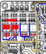
R53 is missing. (T1).
VDR1 (top is wrong). Has to be connected to the top left ~ of the bridge. (See attached)
C3, C4 are missing, but, as you decided, we can live without")
Green, yellow, orange and red LEDS are not supposed to be in board: they are for the front panel of the amp to show the states of protections, reason why i designed them originally on a connector.
I believe it was too complicated.
And the Mosfet IP8025N is a requisite, on my point of view, as it is better than 3 lines of IRF witch was there just as an alternative.
I have still to verify the grounds and power everywhere, and the fans, but i'm confident, reason why i post now: It was a hard work for my eyes ;-)
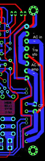
Attached too, suggestion for AC lines.
If i'm not mistaken, there is only very few mistakes.
R53 is missing. (T1).
VDR1 (top is wrong). Has to be connected to the top left ~ of the bridge. (See attached)
C3, C4 are missing, but, as you decided, we can live without
Green, yellow, orange and red LEDS are not supposed to be in board: they are for the front panel of the amp to show the states of protections, reason why i designed them originally on a connector.
I believe it was too complicated.
And the Mosfet IP8025N is a requisite, on my point of view, as it is better than 3 lines of IRF witch was there just as an alternative.
I have still to verify the grounds and power everywhere, and the fans, but i'm confident, reason why i post now: It was a hard work for my eyes ;-)
Attached too, suggestion for AC lines.
Attachments
Last edited:
It appears that you are almost there Christophe. I am glad you did not remove the thread, that would have been very disappointing to you and to everyone following this thread. Now if someone will make some boards or we can produce out own then we are almost there to a wonderful addition to any amplifier.
Steven
Steven
Thanks to sir Alex, and to you for your nice words and you interest.It appears that you are almost there Christophe.
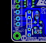
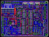
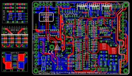
PCB REV 1.4
...... and rev 1.4 printed in b&w and some grey colors to not harm eyes to much .... I will layout so many PCB's , until the final result ,when will be accepted by designer , and all involved in this nice project ....
Regards Alex.
...... and rev 1.4 printed in b&w and some grey colors to not harm eyes to much ....
I will layout so many PCB's , until the final result ,when will be accepted by designer , and all involved in this nice project .... Regards Alex.
Attachments
Only my age and too much time in front of screens are responsible ;-).to not harm eyes to much ...
Please, Alex, take my remarks when i made some as just suggestions: YOU are the master of your designs and a master in this art. I was astonished at each step of verification both by the complexity of the schematic and the imaginative ways you solved the problems.
PCB REV 1.4 REV
...... There were mistakes, I corrected and now I think it's good, what about you? Wiring diagram was not drawn very well in detail, which made me very difficult to route, but finally we managed.We need the final QC .
Regards Alex.
...... There were mistakes, I corrected and now I think it's good, what about you?
Wiring diagram was not drawn very well in detail, which made me very difficult to route, but finally we managed.We need the final QC .Regards Alex.
Attachments
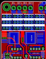
I was verifying the previous version: this is wat i noted, but, may-be you had corrected yet some of them.
C20+R21 missing a connection to next ground.
R43 is missing. I was mistaken, speaking of R53, i apologize. (Base of T1 on my schematic). You can use +17V witch is next, changing R43 value if it helps.
R41 value 200K marked 21K.
I follow with some little suggestions, but you are too fast for me
For the moment, i'm trying to add the IPB025N, seems not too difficult.
When you have questions, please Alex, do not hesitate to ask-me: Big problems of Board design can, sometimes, be changed by a little change in schematic
Take some rest, and we will have the end of the road just near.
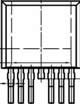
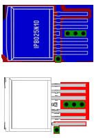
Alex, just a dirty design (i miss the tools): i think it is possible to set the IPB0225N. Attached the body of this piece (I gave you the link to the data-sheet in a previous message.
And the case.
After that, i believe we'll be all finished (You are fantastic, it is an amazing work)
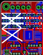
Oh, one more thing, i think it would be better to erase the tracks from R15 R16 to the relay: there is a risk they burn if the user forget to wire the good cables, what do you think ?.
If it is possible, i would like to have an image of the each faces without components, and the components apart. It will help-me for final verification, and to can publish all the various versions with just the needed parts populated, as we did for schematics.
Thanks again to coolet too for his nice help on schematics. We don't forget him.
And the case.
After that, i believe we'll be all finished
(You are fantastic, it is an amazing work)Oh, one more thing, i think it would be better to erase the tracks from R15 R16 to the relay: there is a risk they burn if the user forget to wire the good cables, what do you think ?.
If it is possible, i would like to have an image of the each faces without components, and the components apart. It will help-me for final verification, and to can publish all the various versions with just the needed parts populated, as we did for schematics.
Thanks again to coolet too for his nice help on schematics. We don't forget him.
Attachments
Last edited:
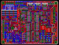
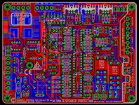
PCB Rev 1.5
What can I say, it's done the last rev 1.5 of PCB . Foot print of power mosfet IRB025N10 was created careful but not feed in place pointed by you dear Christophe .Please send your email on PM to send you all files you need to compare schematic with PCB .
Regards Alex.
What can I say, it's done the last rev 1.5 of PCB . Foot print of power mosfet IRB025N10 was created careful but not feed in place pointed by you dear Christophe .Please send your email on PM to send you all files you need to compare schematic with PCB .
Regards Alex.
Attachments
Last edited:
Oh, one last thing, about power button: The power button IS the bottom AC Switch S202S02. So, if you want ta add a mechanical one instead, the best and simpliest way is to put a connector right in parallel with its two AC poles, using the schematic i provided in post 262.
I did not designed-it because if you need one, it is because you don't had populated the S202S02, so you can wire the cables right in there.
I am not sure to be clear...
But, may-be you had an other idea, like a security power button at the back of an amplifier, like for PC PSUs ?
Attached, a suggestion for mosfets:
Attachments
Last edited:
- Status
- This old topic is closed. If you want to reopen this topic, contact a moderator using the "Report Post" button.
- Home
- Amplifiers
- Solid State
- An ultimate amp protection circuit ?