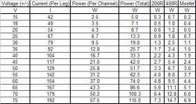
Looking at your graphs, it seems to me that the 35V rails is a good compromise between performance and power consumption. Also because power consumption seems to rise pretty fast with higher rails. I did some quick calculations with the power consumption for four halves - are these correct?
Are you planning to develop the circuit further on 130mA? I'm a bit reluctant to let my DAC dissipate 50W while my power amp idles at 30W...
Code:
V (V)	P (W)		I (mA)
18	11.29		66
25	17.71		80
30	23.17		90
35	29.34		100
40	36.23		110
45	43.85		120
50	52.18		130
75	104.65		180
Are you planning to develop the circuit further on 130mA? I'm a bit reluctant to let my DAC dissipate 50W while my power amp idles at 30W...
Last edited:
Hi Lauret,
I've attached a more detailed voltage/current/power chart which you can reference for any info you might need.
I'm going to proceed with both a 50V and a 25V version, but I'll make sure nobody gets left in the dark. The boards I'm doing will end up being overkill for the lower voltages, but that's not the end of the world. You can always buy the shorter version of the board mount heatsinks and save yourself a few dollars. Worst case, your parts will run cooler.
I'm going to make the board capable of going up to 50V rails, and if you buy the tallest heatsinks, you could probably get up to 70V rails as long as your chassis has good ventilation. Either way though, 100W is probably too much to reasonably expect someone to run their DAC at. I'll provide the flexibility, and let the end user decide.
I'll be using these heatsinks:
Digi-Key - HS374-ND (Manufacturer - 529902B02500G)
They come in 1", 1.5", 2" and 2.5" heights, so people can chose which they want based on how high the rails are going to be. The footprint and board stay the same.
Cheers,
Owen
Attachments
Owen
Very interesting work! Thank you for sharing!
Two questions for you, if you don't mind...
By any chance, would it be possible to position the transistors and power resistors on the edge of the pcb so one has the option of mounting them on a flat aluminum surface (like the bottom of the chassis) for cooling?
Did you get a chance to test the venerable IRF610 for comparison purposes?
Pierre
Hi,
have followed the thread from the very beginning, but haven´t entered till now, to test some things myself and not to discourage anybody.
These simple circuits sound astonishingly well, at least for my taste by far better that any OP-based circuit I came across yet. What bothered me a bit was that measurement values always were rather just acceptable than good, let alone great.
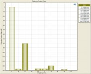
So when I saw the first THD-data from OPC I was really wondering if they could be true. The circuit is a bit parameter sensitive but even with fine tuning, good layouting etc, I never managed to get values better than ~-80dB with a real DAC-output (PCM1794A, Mono-mode) connected to the circuit. The difference to a typical signal source for measurements beeing the rather low output impedance of the DAC-chip´s CCS. Feeding the DAC into a low-ohmic resistor (10-20Ohms) resulted in THD-values better than -100dB. Feeding the I/V-converter from a good signal source gave lower, but nonetheless very good results. Feeding the converter from a real world DAC and nothing better than -80dB resulted (all values referenced to 0dBFS). Those values measured in a circuit with CCS instead of the simple drain- and source resistors used in the D1B1 and a dedicated, rather low valued I/V-conversion resistance (lower values of Ri/v improve THD figures). The simple D1B1 structure redesigned to fit the PCM1794A-DACs resulted in less than -60dB THD+noise. Simple breadboarding showed problems with crosstalk (from the highcurrent paths). Anyway differences of more than 40dB in THD mean that something is wrong. Honestly, THD-values of better than -100dB THD (at fulscale) are unbelievably good for a non-feedback design, while -60dB surely leave room for improvements.
So either the circuit reacts very sensitive to the source it´s fed from or it reacts very sensitive to idle current values or other parameters, or the PCM1794A is a DAC that reacts very sensitive to the load.
Any comments or hints?
jauu
Calvin
have followed the thread from the very beginning, but haven´t entered till now, to test some things myself and not to discourage anybody.
These simple circuits sound astonishingly well, at least for my taste by far better that any OP-based circuit I came across yet. What bothered me a bit was that measurement values always were rather just acceptable than good, let alone great.
So when I saw the first THD-data from OPC I was really wondering if they could be true. The circuit is a bit parameter sensitive but even with fine tuning, good layouting etc, I never managed to get values better than ~-80dB with a real DAC-output (PCM1794A, Mono-mode) connected to the circuit. The difference to a typical signal source for measurements beeing the rather low output impedance of the DAC-chip´s CCS. Feeding the DAC into a low-ohmic resistor (10-20Ohms) resulted in THD-values better than -100dB. Feeding the I/V-converter from a good signal source gave lower, but nonetheless very good results. Feeding the converter from a real world DAC and nothing better than -80dB resulted (all values referenced to 0dBFS). Those values measured in a circuit with CCS instead of the simple drain- and source resistors used in the D1B1 and a dedicated, rather low valued I/V-conversion resistance (lower values of Ri/v improve THD figures). The simple D1B1 structure redesigned to fit the PCM1794A-DACs resulted in less than -60dB THD+noise. Simple breadboarding showed problems with crosstalk (from the highcurrent paths). Anyway differences of more than 40dB in THD mean that something is wrong. Honestly, THD-values of better than -100dB THD (at fulscale) are unbelievably good for a non-feedback design, while -60dB surely leave room for improvements.
So either the circuit reacts very sensitive to the source it´s fed from or it reacts very sensitive to idle current values or other parameters, or the PCM1794A is a DAC that reacts very sensitive to the load.
Any comments or hints?
jauu
Calvin
The D1 stage is mainly 2nd order harmonic typically 80 db down. Disregard that, you can't hear it. Post a 1khz signal tone spectrum picture.
Hi,
have followed the thread from the very beginning, but haven´t entered till now, to test some things myself and not to discourage anybody.
These simple circuits sound astonishingly well, at least for my taste by far better that any OP-based circuit I came across yet. What bothered me a bit was that measurement values always were rather just acceptable than good, let alone great.
So when I saw the first THD-data from OPC I was really wondering if they could be true. The circuit is a bit parameter sensitive but even with fine tuning, good layouting etc, I never managed to get values better than ~-80dB with a real DAC-output (PCM1794A, Mono-mode) connected to the circuit. The difference to a typical signal source for measurements beeing the rather low output impedance of the DAC-chip´s CCS. Feeding the DAC into a low-ohmic resistor (10-20Ohms) resulted in THD-values better than -100dB. Feeding the I/V-converter from a good signal source gave lower, but nonetheless very good results. Feeding the converter from a real world DAC and nothing better than -80dB resulted (all values referenced to 0dBFS). Those values measured in a circuit with CCS instead of the simple drain- and source resistors used in the D1B1 and a dedicated, rather low valued I/V-conversion resistance (lower values of Ri/v improve THD figures). The simple D1B1 structure redesigned to fit the PCM1794A-DACs resulted in less than -60dB THD+noise. Simple breadboarding showed problems with crosstalk (from the highcurrent paths). Anyway differences of more than 40dB in THD mean that something is wrong. Honestly, THD-values of better than -100dB THD (at fulscale) are unbelievably good for a non-feedback design, while -60dB surely leave room for improvements.
So either the circuit reacts very sensitive to the source it´s fed from or it reacts very sensitive to idle current values or other parameters, or the PCM1794A is a DAC that reacts very sensitive to the load.
Any comments or hints?
jauu
Calvin
Hi Guys,
Judging by the last few comments, it looks like mounting the transistors/resistors on the side is the way to go. I guess that way people can either mount them to the bottom of the chassis, or use clip rails and mount heatsinks on either side.
I've moved to TO-220 resistors for the 200 and 400 ohm, and the rest will be both SMD or PTH. I'm still a little torn on the output coupling caps, as I'm not sure how much room to leave for them. Would everyone prefer a little room, lots of room, would you rather wire them off-board (use them as interconnects between the board and the XLR jack)?
I'll be including the regulator section on the board, and I'll be using LM317/337 referenced up as is done in the D1. I'll be running +/-65 VDC unregulated to the board, then regulating down to +/-50 VDC.
As for the 540 and 610, I don't have the 610 here, and the 540 will perform somewhere in the ballpark of the measurements posted here. If someone wants to get me a handful of 610's then I'd be glad to measure them for TC and see how they compare. If it's favorable, then I might also measure them in circuit and see how they perform.
Calvin:
Sounds like you've done a lot of work, which is very good to see! There are a few issues with the measurements you're getting, and I'll try to cover them below:
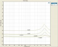
1. The measurements posted in the first post are at -10dBFS. When you run the circuit at +/-18V the THD+N curve has a null at -10dBFS and then rises above that. If you want to get better than -100dB THD+N at 0dBFS, then you'll need to go to higher rails. For the buffalo II, you get decreasing distortion right up to 0dBFS with 45V rails or higher. Take a look at the most recent THD+N measurements taken at different voltages. You'll see the curve I'm talking about on the lower voltage rail variants.
2. You'll need to post the circuit you're using, along with what output voltage you're getting when you're at 0dBFS. I don't know what the output current is on the PCM1794 in mono mode, but I'm going to guess it's pretty high. If it is higher than the buffalo, then you have the luxury of reducing the gain (dropping the 200 and 400 ohm resistors even lower) until you get 2VRMS output. If you do that, and bump the rails up a little, I'm positive you'll get better than -100dB THD+N.
3. What devices are you using for the mosfets? Are the supplies regulated? Are you using separate supplies for both left and right channels? I've not had any problems with crosstalk so I'm surprised to hear that.
4. Can you post your measurements so we can take a look?
Cheers,
Owen
Judging by the last few comments, it looks like mounting the transistors/resistors on the side is the way to go. I guess that way people can either mount them to the bottom of the chassis, or use clip rails and mount heatsinks on either side.
I've moved to TO-220 resistors for the 200 and 400 ohm, and the rest will be both SMD or PTH. I'm still a little torn on the output coupling caps, as I'm not sure how much room to leave for them. Would everyone prefer a little room, lots of room, would you rather wire them off-board (use them as interconnects between the board and the XLR jack)?
I'll be including the regulator section on the board, and I'll be using LM317/337 referenced up as is done in the D1. I'll be running +/-65 VDC unregulated to the board, then regulating down to +/-50 VDC.
As for the 540 and 610, I don't have the 610 here, and the 540 will perform somewhere in the ballpark of the measurements posted here. If someone wants to get me a handful of 610's then I'd be glad to measure them for TC and see how they compare. If it's favorable, then I might also measure them in circuit and see how they perform.
Calvin:
Sounds like you've done a lot of work, which is very good to see! There are a few issues with the measurements you're getting, and I'll try to cover them below:
1. The measurements posted in the first post are at -10dBFS. When you run the circuit at +/-18V the THD+N curve has a null at -10dBFS and then rises above that. If you want to get better than -100dB THD+N at 0dBFS, then you'll need to go to higher rails. For the buffalo II, you get decreasing distortion right up to 0dBFS with 45V rails or higher. Take a look at the most recent THD+N measurements taken at different voltages. You'll see the curve I'm talking about on the lower voltage rail variants.
2. You'll need to post the circuit you're using, along with what output voltage you're getting when you're at 0dBFS. I don't know what the output current is on the PCM1794 in mono mode, but I'm going to guess it's pretty high. If it is higher than the buffalo, then you have the luxury of reducing the gain (dropping the 200 and 400 ohm resistors even lower) until you get 2VRMS output. If you do that, and bump the rails up a little, I'm positive you'll get better than -100dB THD+N.
3. What devices are you using for the mosfets? Are the supplies regulated? Are you using separate supplies for both left and right channels? I've not had any problems with crosstalk so I'm surprised to hear that.
4. Can you post your measurements so we can take a look?
Cheers,
Owen
Just a thought .... the THD of the Sabre in Vout configuration is -108dB, Iout is 120dB. In order to make it worthwhile using an I/V stage, surely it's necessary to make THD better than 108dB.
No the pass D1 stage have sonice that are special beyond simple THD measurments.
If you want good measurements on paper stick to opamps.
No the pass D1 stage have sonice that are special beyond simple THD measurments.
Have you compared the sonics of the Sabre in Vout to Iout mode?
If you want good measurements on paper stick to opamps.
I'm personally not that concerned about ultra low THD .... what I'm asking is what benefit there is going through I/V at all if one is not concerned about measurements.
Hi Spartacus,
Not a bad question... I'll try it today both measured and listening. From my simulation a 190 ohm resistor on each leg should give about 2VRMS output, so I'll start there.
Regards,
Owen
Hi Owen, look forward to hearing your results!
Dan
Have you compared the sonics of the Sabre in Vout to Iout mode?
I'm personally not that concerned about ultra low THD .... what I'm asking is what benefit there is going through I/V at all if one is not concerned about measurements.
-Study up on Nelson Pass theory. NFB = Bad. 2nd harmonic distortion = almost inaudible. THD does not evaluate a circuit. I'll take an 80db THD w/ predom 2nd order distortion over a 110db THD predom high order distorion w/ NFB on my DAC any day of the week.
-Study up on Nelson Pass theory. NFB = Bad. 2nd harmonic distortion = almost inaudible. THD does not evaluate a circuit. I'll take an 80db THD w/ predom 2nd order distortion over a 110db THD predom high order distorion w/ NFB on my DAC any day of the week.
Hi Regal, thanks for your response. I'm aware of such ideas, but they are irrelevant to the question I was raising.
I'm asking why have an I/V at all if the Sabre chip is already capable of providing a voltage output with low THD. In fact, the only reason I can think of for going the I/V route is if one wants the -120dB THD the Sabre chip is capable of in that mode, but then isn't that only worth doing if the I/V converter itself has a similarly low THD? Do you see?
I'm open minded - there may be other mechanisms going on. However Vout mode also has the benefit of reduced modulation of the DAC's power supply, and we all know how sensitive the Sabre is here.
Last edited:
The school of thought I'm in is that high open loop gain high NFB is bad in a DAC analog stage.
When you use the Sabre V-out mode you are just using its internal opamps. If thats your direction fine, but it has nothing to do with Nelson's genius D1 stage.
When you use the Sabre V-out mode you are just using its internal opamps. If thats your direction fine, but it has nothing to do with Nelson's genius D1 stage.
Hi Regal, thanks for your response. I'm aware of such ideas, but they are irrelevant to the question I was raising.
I'm asking why have an I/V at all if the Sabre chip is already capable of providing a voltage output with low THD. In fact, the only reason I can think of for going the I/V route is if one wants the -120dB THD the Sabre chip is capable of in that mode, but then isn't that only worth doing if the I/V converter itself has a similarly low THD? Do you see?
I'm open minded - there may be other mechanisms going on. However Vout mode also has the benefit of reduced modulation of the DAC's power supply, and we all know how sensitive the Sabre is here.
The school of thought I'm in is that high open loop gain high NFB is bad in a DAC analog stage.
When you use the Sabre V-out mode you are just using its internal opamps. If thats your direction fine, but it has nothing to do with Nelson's genius D1 stage.
But the Sabre has no internal op-amps, no negative feedback. Using it in V-out mode doesn't necessitate using any extra circuitry/NFB at all. You can connect it's output directly to an amplifier input (with a DC blocking capacitor if needed), and if you believe in simple is best, this is obviously the way to do it.
So, why use an I/V stage at all? Most people do so because you get a few dB lower distortion. But if you don't care about super low distortion, what's the point? There may be a point somewhere, and I'm happy to hear any ideas.
Last edited:
Hi Spartacus,
Well, I think this should be a lesson in trusting datasheets, especially those with unqualified distortion numbers.
The ESS datasheet does indeed specify -108dB THD+N in voltage mode, but there's not much more data there. I'd ask the following:
- At what output voltage?
- At what frequency?
- With what HF and LF noise filters?
- With what value of resistor?
- With what circuit following the output?
I started with a pair of 200 ohm resistors, but that only gave me 1VRMS output. I ended up with 750 ohm resistors which was giving me 1.75VRMS output. Still not high enough to be a fair comparison to the circuit I'm using.
The following THD+N graphs were measured the exact same way as I've been measuring the circuit I've been working on. Same Buffalo 32 DAC, same channel, 192kHz, 24 bit.
The best I could get was -102dB THD+N but that was only at 1kHz and only at -13 dBFS. At 0 dBFS you're looking at closer to -80dB THD+N best case.
I'm not sure how they got the numbers they did... maybe you need an op-amp buffer, maybe they have an actual circuit that counts as "Voltage Mode" but you're not going to get that kind of performance with just resistors. Worse yet, almost all the distortion is 3rd order, which means there's probably large amounts or second order if you don't run balanced outputs. If anyone out there is using this single-ended with a resistor in voltage mode, then you're probably getting terrible results. This is part of the reason you should never design solely "by ear".
To answer your initial question, the IV stage buys us 30dB better distortion and lower output impedance. That's the point in using it.
Always be wary of THD+N measurements when there's no circuit, no graph, and no other measurement data than a single number.
Cheers,
Owen
Attachments
But the Sabre has no internal op-amps, no negative feedback. Using it in V-out mode doesn't necessitate using any extra circuitry/NFB at all. You can connect it's output directly to an amplifier input (with a DC blocking capacitor if needed), and if you believe in simple is best, this is obviously the way to do it.
So, why use an I/V stage at all? Most people do so because you get a few dB lower distortion. But if you don't care about super low distortion, what's the point? There may be a point somewhere, and I'm happy to hear any ideas.
I'll have to read that white paper again I thought all V-out DAC's had internal opamps.
- Status
- This old topic is closed. If you want to reopen this topic, contact a moderator using the "Report Post" button.
- Home
- Source & Line
- Digital Line Level
- A New Take on the Classic Pass Labs D1 with an ESS Dac