I have no idea if the network I posted would be the 'optimal' from a generic point of view. I arrived at these values through a lot of experimental testing. Zobels are generally 10R/100n. But I found this to be affecting high frequency THD and reduced the capacitor to 47n to make its impact neglible THD wise (the THD junkie I am). For the output coil I at first used the generic 1uH, but found that I could lower it to 500n just fine without compromizing stability. The shunt R generally is 10R, but I found that lowering it to 2R2 makes THD20K immune to the R//L combination with a 4R load while retaining enough series resistance for a pure capacitive load. Which I also added to the output network for stability purposes. I tinkered my schematic's compensation against this 22nF pure load and it appears to ensure a steady PM/GM in the full capacitive range up to 2u (didn't go further because of execessive loading at HF)My question is, how do you optimize the values of each of the components in that diagram? With such a complex output filter there are so many variables, how do we know if it's optimal?
But I wouldn't go out and say that the configuration I posted would be suited for every circuit. But it's a starting point I suppose. As for interaction, given that the OPS under normal conditions has almost a zero output impedance I don't think there's much inter-dependant interaction.
But who am I? I find myself simming endlessly instead of building
 I just want to try to get things right as much as I can before starting the big prototype.
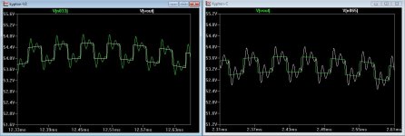
Hi dadodWhen I look at the graph, the squares seem to have peak-to-peak value of about 5V instead of .2? Also, is that without input filter?
Input was set to+-100mV square times the gain and you get +-3V. Maybe this is to much to ask from the amp?? That was with input filter.
Hey keantoken, I don't know who you were referring to but the guy I was looking for posted in this thread and in this one and he's been mia since the summer. Has someone else taken up his cause?
Last edited:
Ah okay, I was just wondering, as Keantoken was speaking of +-100mV at the output and not the input. I don't think you're asking too much from the amp, the graph looks very peachyInput was set to+-100mV square times the gain and you get +-3V. Maybe this is to much to ask from the amp?? That was with input filter.
 .
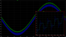
.Simming that 100Hz/20KHz wave indeed takes VERY long but I did it, using a pure 2u load (no parallel R). Warning, it's a big picture. The blue graph is the output after the inductor, the green before the inductor. I deliberately offset the blue graph by 10 volts to separate the waves. I also added a close-up of part of the wave where I did not offset the waves to keep them overlapping.
Attachments
I think that 100Hz sin and 20kHz square is to extreme, it takes to long to run simulation.
Here is 2kHz sin at almost full power and 20kHz square +-100mV from my lateral MOSFET 200W amp.
Be patient.
MagicBox said:Here is an example of a "complete" output network.
My main incentive for looking at Cherry's simplified output network was the possibility of getting rid of 1 large 10R resistor.[*]Yes, excellent. One further point. I sometimes recommend a "distributed" on-board Zobel consisting of several smaller Zobels close to each output pair when multi-pair output stages are used. This enables the use of smaller Zobel components and non-inductive metal-oxide or metal-film resistors. Fast output transistors like to have the Zobels close-by. This approach does not necessarily take up much more PCB space.
Simple sims show excellent results but the savings may not be realised in 'real life'.
In 'real life', these networks MUST be close to the output stage. The inductance of tracks & wiring is enough to make the simple Cherry network unusable with the usual wiring to the speaker terminals.
You could put the Cherry network on the PCB so its close to the output stage with well defined proximity & strays but then the Inductor is close to yucky high current PSU lines.
The best general solution might be
- Bob's individual Zobels (which I believe are directly on the output emitters (rather than at the junction of the emitter resistors)
- then the Inductor/Resistor which can be situated somewhere which doesn't pick up yucky EM fields
- 22n ceramics on the speaker terminals and perhaps also from each speaker terminal to chassis so it gets rid of RFI coming in via the speaker leads.
___________________
Bob, I think Thiele suggested the present Zobel + Inductor/Resistor network in the 60's. It wasn't new then. I'm just using Self's terminology (which calls the Inductor/Resistor "Thiele") .. eg like "Blameless" which certainly wasn't new when Self hijacked it.
[*]If this sounds like I'm anal about 1 resistor, that's cos I am
On the resistors....How about "inductive" vs non - "inductive" and SMD and thru hole. And throw in SMD caps vs thru hole to along with where they are mounted. Double side vs single sided boards with and with out ground planes. And last but not least BJT vs FET. And the FET's with and without internal protection. Can you hear the difference let along measure it.
Simple sims show excellent results but the savings may not be realised in 'real life'.
But all this needs extensive testing in 'real life'.
For myself, this is the point were I have invested in test equipment. I started with SIM and still have a fairly good one (same one D.Self uses) but you cant go to advanced build stage without good test equipment.
THx-RNMarsh
Last edited:
I have no idea if the network I posted would be the 'optimal' from a generic point of view.
I find myself simming endlessly instead of building
When you are done with sim you have to prototype and test/measure; Adjust as needed from results.
[ At least for non-corporate developers (DIY) without the tools to do more complete sim's all the way to production.]
Is there really any other way to know for certain?
THx-RNMarsh
Last edited:
That's the process I followed with my MF80 80W/4R mosfet design. It was/is a fully symmetrical complementairy circuit with cascoded darlington VAS stage. I developed it in Multisim and when I felt it was ready I went ahead, designed the board, got the components and built itWhen you are done with sim you have to prototype and test/measure; Adjust as needed from results.
[ At least for non-corporate developers (DIY) without the tools to do more complete sim's all the way to production.]
Is there really any other way to know for certain?
THx-RNMarsh
The only difference between reality and sim was in the Vbe of the BC550C's I was using, ending up with a too large VAS current. I adjusted back to what it had to be by adjusting the emitter resistors (from 22 to 33r) and reflected this back to the simulator, also updating the models as I got better models. This went back and forth a few times and the result was an amp that measured (soundcard) MUCH better than Multisim suggested! I've posted a reference to this little project some time ago; on a Dutch forum though. I'm still very much proud of the little amp; it has wonderful sound. MMMmmmosfets This project showed me though, that you'll Always keep tinkering even if you think you're done. That's why I want to delay building the big prototype I'm working on now as much as possible. I just KNOW that I want to add this or that, or improve this or that after having sent in the gerbers lol. I want to avoid that haha.
Last edited:
The only difference between reality and sim was in the Vbe of the BC550C's I was using, ending up with a too large VAS current. I adjusted back to what it had to be by adjusting the emitter resistors (from 22 to 33r) and reflected this back to the simulator, also updating the models as I got better models.
Design "slop factor" into the circuit. If you see you have different currents
with multiple models , add a trimmer to the CCS or to some point which
will allow adjustment of the circuits basic operating points.
Builders will use whatever they have in the "junkbox"
.For CFA's this would mean 2 trimmers ... builders ask too many questions
with this arrangement. Just find some other point in the circuit
that will give a (symmetrical) final adjustment
(hawksford VAS LED current - for example).
OS
Ah okay, I was just wondering, as Keantoken was speaking of +-100mV at the output and not the input. I don't think you're asking too much from the amp, the graph looks very peachy
Simming that 100Hz/20KHz wave indeed takes VERY long but I did it, using a pure 2u load (no parallel R). Warning, it's a big picture. The blue graph is the output after the inductor, the green before the inductor. I deliberately offset the blue graph by 10 volts to separate the waves. I also added a close-up of part of the wave where I did not offset the waves to keep them overlapping.
That's a real cool torture test ... some amps don't do as well as others.
Transient analysis took 5 sec (instant is normal)
"fast ones" (amps) seem to like it.
thanks !
OS
Attachments
For myself, this is the point were I have invested in test equipment. I started with SIM and still have a fairly good one (same one D.Self uses) but you cant go to advanced build stage without good test equipment.
THx-RNMarsh
100% agree. My set of equipment is not as comprehensive as yours, but gives enough accuracy for understanding what's going on and keeping things under control. Spectrum analyser is very important. I would be "blind" without it
And yes - we only know for sure, as soon as it's live-prototyped. Even having a lot of experience with simulations - we come close to reality - but there are aways some nuances, not covered by the model, but still important ones.
That's a real cool torture test ... some amps don't do as well as others.
Transient analysis took 5 sec (instant is normal)
"fast ones" (amps) seem to like it.
thanks !
OS
This is cool
My main incentive for looking at Cherry's simplified output network was the possibility of getting rid of 1 large 10R resistor.[*]
Simple sims show excellent results but the savings may not be realised in 'real life'.
In 'real life', these networks MUST be close to the output stage. The inductance of tracks & wiring is enough to make the simple Cherry network unusable with the usual wiring to the speaker terminals.
You could put the Cherry network on the PCB so its close to the output stage with well defined proximity & strays but then the Inductor is close to yucky high current PSU lines.
The best general solution might be
But all this needs extensive testing in 'real life'.
- Bob's individual Zobels (which I believe are directly on the output emitters (rather than at the junction of the emitter resistors)
- then the Inductor/Resistor which can be situated somewhere which doesn't pick up yucky EM fields
- 22n ceramics on the speaker terminals and perhaps also from each speaker terminal to chassis so it gets rid of RFI coming in via the speaker leads.
___________________
Bob, I think Thiele suggested the present Zobel + Inductor/Resistor network in the 60's. It wasn't new then. I'm just using Self's terminology (which calls the Inductor/Resistor "Thiele") .. eg like "Blameless" which certainly wasn't new when Self hijacked it.
[*]If this sounds like I'm anal about 1 resistor, that's cos I am
Might there be a reference somewhere with regard to Theile coming up with that network in the '60s? I'd be interested. I missed it that Self tagged it. Did he give a reference? I don't recall him using the term in any of his earlier editions.
Regarding distributed Zobels, I did not actually have in mind a separate Zobel for the NPN and PNP devices, rather just one Zobel per output pair, distributed along the output rail. Interesting thought, though, about using them connected directly to the emitters.
Cheers,
Bob
Hi Bob,
There's an article on AES - >Load Circuit Stabilizing Networks for Audio Amplifiers<. I've got a copy, purchased from there.
But it's not really '60s - February 1976...
Cheers,
Valery
Regarding distributed Zobels, I did not actually have in mind a separate Zobel for the NPN and PNP devices, rather just one Zobel per output pair, distributed along the output rail. Interesting thought, though, about using them connected directly to the emitters.
Cheers,
Bob
Hi Bob,
Did you mean something as this. My 200W CFA with VMOSFET OPS.
BR Damir
Attachments
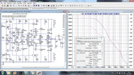
Did you mean something as this. My 200W CFA with VMOSFET OPS.
I proposed this a while back and asked for comments >HERE< and >HERE< because it seems obvious but I hadn't previously seen it.
Edmond Stuart had previously replied that it made sense to him.
Nice to see you have also (re)invented it, another valued opinion makes me even more reassured.
I hope to have Bob's assessment too, this time.
Best wishes
David
Last edited:
There's an article on AES - >Load Circuit Stabilizing Networks for Audio Amplifiers<. I've got a copy, purchased from there.
But it's not really '60s - February 1976...
Some of Thiele's work was published first in Australia in the '60s, then republished in the '70s in journals with more international circulation, after it's importance was eventually realized by the rest of the world.
But this one was only published one year earlier in Australia, 1975.
I suppose that's closer to the '60s, or perhaps the date has been confused with the other material.
Best wishes
David
Last edited:
I use one zobel it goes from the point where i take tthe speaker out from the PCB and to the main star GND on the PCB where also the speaker GND wire is connected.
Cant possibly see what multiple smaller value zobel's should provide of benefits, only reason could be the possible use of non-inductive resistors. I believe that issues with HF return ingress should be dealt with right where it enters and should be shunted to the point of lowest possible GND impedance.
Cant possibly see what multiple smaller value zobel's should provide of benefits, only reason could be the possible use of non-inductive resistors. I believe that issues with HF return ingress should be dealt with right where it enters and should be shunted to the point of lowest possible GND impedance.
Last edited:
- Home
- Amplifiers
- Solid State
- CFA Topology Audio Amplifiers