Did you ever planned or make that crossconnection transistors to not switched off and work inclass AB instead,
I've tried it, no result.
May be with miralin Re implementation, I am going to use cross management in it, so bias rises to make output transistor not switched off. But I am too busy now, finishing my new mini mixers.
Hi Edmond&friends
Congratulations and Happy New Year!
Hope in 2012 we’ll have pleasure to talk about basic principles, nonlinearities, etc.
Cheers Mir
Hi Mir and all other DIYers,
A happy and prosperous New Year.

Edmond.
Did you ever planned or make that crossconnection transistors to not switched off and work inclass AB instead, I just have this idea and not yet tried it.
I've tried it, no result.
May be with miralin Re implementation, I am going to use cross management in it, so bias rises to make output transistor not switched off. But I am too busy now, finishing my new mini mixers.
Hi ontoaba,
Class-I as well as AB2 comprise two NFB loops:
1. A common-mode loop, that controls the bias of the OPS
2. A differential loop, that minimize the distortion of the OPS.
Regarding the 1st loop, it's essential that this loop is highly nonlinear, I repeat highly nonlinear. That means that one or more bias controls trannies will be and have to be switched off during large output currents.
Anny attempt to linearize the bias FB loop clearly demonstrates nothing but a lack of proper understanding of the basic principles of these circuits.
Regarding the 2nd loop, indeed this one needs to be linear. In the AB2 circuit, this has already been achieved by using a 'reversed' CFB stage, which is inherently quite linear. I call it 'reversed' as the amp output is fed to the input of this CFB stage and and the amp input is connected to the feedback point of this stage.
I'm still busy with my 'explanation', as it's getting quite long. Perhaps I don't put it here, rather on my own website, because 'over there' I can add or correct things at any time. Till then, please no more so called 'improvements', but feel free to put any question.
Success with your mini mixers.
Cheers,
E.
Last edited:
Hi ontoaba,
Class-I as well as AB2 comprise two NFB loops:
1. A common-mode loop, that controls the bias of the OPS
2. A differential loop, that minimize the distortion of the OPS.
Regarding the 1st loop,.... I repeat highly nonlinear..
......
Ok, no more improvement, it is my OPS that need to be improved, because your AB2 works much better with my XM, around 1mV spikes
 .
.Thanks , my mini mixer now in build progress (PCB drilling).
Attachments
About reversed CFB, I am using it cut cascoded (also work like this with AB2) and with resistor replacing current source in most my EC, its stable negative feedback with shortest feedback path.
Finished with drilling, I trying to place 2nd storage XM, and it is also work great.
Ok, Kendall class-I is just same with nakayama's circuit or kendall is nakayama?. I see pioneer M91 amplifier also using non switching IC, but don't know what it is.
Finished with drilling, I trying to place 2nd storage XM, and it is also work great
.Ok, Kendall class-I is just same with nakayama's circuit or kendall is nakayama?. I see pioneer M91 amplifier also using non switching IC, but don't know what it is.
Attachments
Last edited:
Ok, no more improvement, it is my OPS that need to be improved, because your AB2 works much better with my XM, around 1mV spikes
Thanks , my mini mixer now in build progress (PCB drilling).
I don't get spikes at all, only a tiny wobble that resembles the distortion caused by gm doubling. Moreover, if I replace the switching sense trannies by something that doesn't switch at all (for example a multiplier) I get almost exactly the same results.
edit: So the switching sense trannies have nothing to do with your spikes.
If you get spikes then something is fundamentally wrong, either your schematic or your simulator.
Cheers,
E.
Last edited:
Good research, Walter !
So the late Baxandall (RIP) is not the father of that baby.
Bottom line: everything you invent has already been invented.
Oh well.
Cheers,
E.

Hi Edmond
The granting of this new patent is like a joke, the author has even patented outputstage inclusive miller compensation which has and is widely used. As TMC was patented before and is public knowledge this patent should never have been granted.
Watch out guys, I might just get the nerve to go patent miller compensation or even better Negative feedback again.
Ive been testing TMC with the LM chips for a cheap new range of automotive amps using TMC the last few days and so far results look good. I about to start preparations to commercialize and I wish Mr Zhenwu Wang all the best of luck if he decides to sue to me.
About reversed CFB, I am using it cut cascoded (also work like this with AB2) and with resistor replacing current source in most my EC, its stable negative feedback with shortest feedback path.
Finished with drilling, I trying to place 2nd storage XM, and it is also work great
Ok, Kendall class-I is just same with nakayama's circuit or kendall is nakayama?. I see pioneer M91 amplifier also using non switching IC, but don't know what it is.
I might be able to help here, Pioneer do have a patent but they also used the circuit in a discreet implementation in a amp or two. Ill try post the circuit if Edmond and DAdod dont mind as its offtopic.

I might be able to help here, Pioneer do have a patent but they also used the circuit in a discreet implementation in a amp or two. Ill try post the circuit if Edmond and DAdod dont mind as its offtopic.
I don't mind (as we are already off topic), so please proceed.
Cheers,
E.
I don't get spikes at all, only a tiny wobble .....
If you get spikes then something is fundamentally wrong, either your schematic or your simulator.
.....
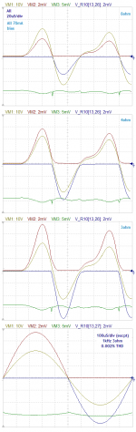
Sorry I am not explain before, that I am using less than 50mA (just30or20) bias and lower the loop gain at HF for stability, so the spike normally appeared. There also no significant spike at 100mA or higher bias.
Looks like that hitachi patent used for HAxxxxx IC, and sadly they sound not good enough, in other side LA4xxx from sanyo using common simpler technique with much better to hear. Wrong technique that been patented, just a waste. I agree that the patent isn't worth.
I see that pioneer IC similar with kendall classI, don't know for sure.
Spikes
>I am using less than 50mA (just 30 or 20) bias
Hey man, that's Class-B. No wonder you get spikes.
For two reasons that doesn't work, or at least far from optimal:
1. It's generally agreed that MOSFET OPSes should be operated in class-AB. That means a quiescent current of at least 100mA (150mA is a good compromise between low distortion and excessive heat production).
2. Auto bias circuits (Class-I, AB2, LT1166 etc) are based on the so called geometric mean concept. IOW, they try to keep the product of the P and N channel FET currents at a constant level. You can't use this technique for class-B output stages; only for class-AB. Why?
Suppose Iq = 30mA and the maximum current is 3A (100 times more). That means -for a constant product- that the trannie(s) of the other gender should draw 30mA/100 = 0.3mA. This tiny current times a typical sense resistor of say 0.33 Ohm gives 0.1mV.
A simple circuit built around a few discrete poorly matched trannies can never handle such small a voltage with sufficient accuracy. An ideal precision multiplier might handle it, but only at low frequencies. Above 100Hz or so, capacitive effects (gain roll-off etc) affect the accuracy too much and the circuit goes berserk, i.e. spikes.
Now, suppose Iq = 150mA and the maximum current is (again) 3A, i.e.20 times more. In this case the current through the other tranny is 150mA/20 = 7.5mA, being 25 more than in the previous case and it gives 2.5mV across the sense resistors. With reasonable matched trannies this voltage is manageable. But to be on the safe side (the circuit should work under a wide range of temperatures and components tolerances), I even prefer a much higher minimum current in the order of 50mA. As a result, no spikes at all and a much lower distortion. Happily, you already figured that out by yourself.
Cheers,
E.
edit: NB, in Kedall's class-I BJT OPS the bias current is 135mA.
Last edited:
Product
Hi Edmond
Some ten years ago I’ve analyzed a circuit that is now called “Class-I” (don’t know why – maybe ask Mr.Nakayama?). This cirquit (unlike the most of other nonlinear ones) yields to precise mathematical analysis without simulations or approximations. The result shows that the product (Ip*In) is not constant. The relationship is slightly more complex.
Can’t say anything about other circuits. May be your simulation software can plot the product against output current like the currents themselves in Fig.8 of your basic “AutoBias_II.html” for those and new variants. I’m especially interested of your ingenious crossconnection solution.
Cheers Mir
PS. I think that either precondition on or relationship between Ip&In will disturb the main condition:
Ip-In=G*Vin, where resulting transconductance G is constant (except those which are the consequences of this condition).
Thanks for useful explanations, I am, just showing there, it fit with XM better than my OPS. In this case, current sense isn't just resistor, nor just diode/schottky, but it has special arrangement of some components.
Hi, Edmond, can't it modified to something that not need transistor matching? Because pioneer that uses special IC also sometimes one channel perform right, and other channel just worse.
Pioneer has 204mA bias.
Hi, Edmond, can't it modified to something that not need transistor matching? Because pioneer that uses special IC also sometimes one channel perform right, and other channel just worse.
Pioneer has 204mA bias.
Hi Edmond
Some ten years ago I’ve analyzed a circuit that is now called “Class-I” (don’t know why – maybe ask Mr.Nakayama?).
Hi Mir,
Kendall Castor-Perry was the man who dubbed it Class-I. I'm not sure who's the first inventor, he or Nakayama, though I think it was Kendall.
This circuit (unlike the most of other nonlinear ones) yields to precise mathematical analysis without simulations or approximations. The result shows that the product (Ip*In) is not constant. The relationship is slightly more complex.
Can’t say anything about other circuits. May be your simulation software can plot the product against output current like the currents themselves in Fig.8 of your basic “AutoBias_II.html” for those and new variants.
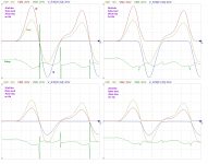
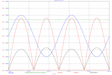
You're right. The relation is more complex and the product isn't really constant. That's why I've said that the circuit only approximates a constant product or tries to keep it constant. Regarding the AB2 circuit as posted on this forum, this one behaves the same as depicted by fig.8 on my website. The pictures below, black curve, shows the product. As you see, far from constant. The main reason is that the minimum Ie has been considerably elevated to 40mA on purpose (for safety reason).
I’m especially interested of your ingenious cross-connection solution.
Cheers Mir
The cross-connection reduces the feed-through of switching currents (of the sense trannies) into the main signal path. As a result, less induced distortion from these trannies. However, it has hardy any effect on the Ip*In product.
PS. I think that either precondition on or relationship between Ip&In will disturb the main condition:
Ip-In=G*Vin, where resulting transconductance G is constant (except those which are the consequences of this condition).
That's a very good point. Also Damir put a (related) question about this subject. For a BJT OPS there exist the so called Barny Oliver optimum point (26mV across both emitter resistors), which provide a more-or-less constant gm over the whole range of output currents.
The schematic on page 41 however, seems to violate this rule, as the sum of voltages across R35 & R36 is much higher: 66mV. That means gm doubling, isn't it? Nope! Apparently, it's all a matter of definition. In this case we should define Vin as the mean voltage of the top and bottom driver input. Thus Vin = 0.5 * ( V(B1) + V(B2) ) and the ouput current is I(R37).
So the incremental transconductance becomes: gm = del( I(R37) / del (0.5 * ( V(B1) + V(B2) ) - V(out) )
To my own surprise, gm is almost perfectly constant. At Vout =0 there is a tiny dip of about 2.7%. No gm doubling at all. See the green curve.
In case of a MOSFET output stage, the picture is quite different. There is no optimal bias point, with or without auto bias. Gm gets reasonably flat at only a very impractical Rs of 1 Ohm or more and a bias current of at least 1A. With Rs=0.22 Ohm and Iq = 150mA my simulation shows a gm variation of about 1:3. Except class-heat, I'm afraid there's nothing we can do about it.
Cheers,
E.
Attachments
That's a very good point. Also Damir put a (related) question about this subject. For a BJT OPS there exist the so called Barny Oliver optimum point (26mV across both emitter resistors), which provide a more-or-less constant gm over the whole range of output currents.
The schematic on page 41 however, seems to violate this rule, as the sum of voltages across R35 & R36 is much higher: 66mV. That means gm doubling, isn't it? Nope! Apparently, it's all a matter of definition. In this case we should define Vin as the mean voltage of the top and bottom driver input. Thus Vin = 0.5 * ( V(B1) + V(B2) ) and the ouput current is I(R37).
So the incremental transconductance becomes: gm = del( I(R37) / del (0.5 * ( V(B1) + V(B2) ) - V(out) )
To my own surprise, gm is almost perfectly constant. At Vout =0 there is a tiny dip of about 2.7%. No gm doubling at all. See the green curve.
Cheers,
E.
Hi Edmond,
I stated that Barny Oliver optimum point is 26mV across one emittor resistor(plus re of the transistor) not both emitter resistors, so you are not so far of it.
Damir
VT
Hi Damir,
You are right: 26mV across one emitter resistor. That was a stupid mistake, sorry (I was misled by D. Self who defined Vq as the sum of both voltages).
With 26mV across each of the emitter resistors (and keeping Iq equal), distortion drops by 10-20%.
Cheers,
E.
Hi Damir,
You are right: 26mV across one emitter resistor. That was a stupid mistake, sorry (I was misled by D. Self who defined Vq as the sum of both voltages).
With 26mV across each of the emitter resistors (and keeping Iq equal), distortion drops by 10-20%.
Cheers,
E.
Last edited:
VT
Hi Damir,
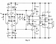
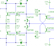
It appears to be quite simple to lower the voltage across the emitter resistors to just 26mV. I was afraid that it should compromise the temperature stability, but that wasn't the case. It's even slightly better, see table.
Simply insert two 3.9R resistors (R38 & R39) as shown below and decrease RE from 0.33 to 0.25R.
Cheers,
E.
Hi Damir,
It appears to be quite simple to lower the voltage across the emitter resistors to just 26mV. I was afraid that it should compromise the temperature stability, but that wasn't the case. It's even slightly better, see table.
Simply insert two 3.9R resistors (R38 & R39) as shown below and decrease RE from 0.33 to 0.25R.
Code:
Ta (C)  Iq (mA)
0       105.4
25      105.4
50 106.4E.
Attachments
The Barny Oliver optimum point
For those who prefer an optimal bias current over a larger temperature range, make R8=R9=R11=R12=1Ohm and adjust the current sources to get an Iq of 100mA at room temperature again (page 41, R7=R10=107 Ohms). Now Iq is proportional to the abs. temp. so that the voltage drop across the emitter resistors equals the thermal voltage VT=kT/q.
Cheers,
E.
What about R38 and R39, not needed??
Damir
- Status
- This old topic is closed. If you want to reopen this topic, contact a moderator using the "Report Post" button.
- Home
- Amplifiers
- Solid State
- Class i and siblings