post257.
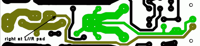
The NFB tapping should be from the same output pad as the Output L//R.
BTW,
I think it is better to mount the L//R off the PCB and put it in the route from PCB to speaker terminals. Keep the Zobel C+R very close to the output devices.
Andrew , why did you not advise Quasi to do that ?? (post 254 , picture 2). As a project I am already at 2 boards per amp ... no external L//R. I can still do the NFB routing , heck I will , just to put this to sleep AND be better than the others.
This leaves me with a choice with the PB250 , which is worse taking NFB from halfway between 2 opposing outputs where I do now or running a real long trace right to the output pad. A way around this actually would be to run a grounded shielded wire right from the NFB input of the voltage board directly to the L//R pad , bypassing all the board contamination.
OS
Last edited:
See pix 1 below and tell me how the signal would be different from the present NFB point or the pad with this style layout. I won't argue the point .. as I will document AND add 1 more pad to run a shielded NFB from the present jumper to the L//R pad (method 2). ")
Pix 2 is the PB 60 , absolute NFB takeoff , right at the pad.... shorter route.
OS
Pix 2 is the PB 60 , absolute NFB takeoff , right at the pad.... shorter route.
OS
Attachments

Last edited:
If you run the shielded wire just tack the ground shield to the voltage board ground connection on just 1 end of the wire . I did this on the first "frugalamp" (like the AX) no problems.Ostripper, when you run that wire, what node should the shield be connected to?
Also, the 220pF input cap makes me nervous. What if you get a high source impedance?
- keantoken
I am running the 220p on the "supersyms" now, no problems. On both the "supers" and these new ones , the input is shunted by a 100k resistor between the input and signal ground.
Do you see my point on the NFB , Kean. The middle of the op trace is the "fulcrum" for the opposing voltages coming through the emitter resistors .. each 40mm spacing between each p / n emitter pair is a separate amp in itself . To put the shield right to the L//R trace IS better , I agree ... but only by a VERY small degree. On a typical left - right layout (actual traces meeting at a center point) , going off-center by even a few millimeters can be seen as corruption and a bad choice for a takeoff point. I have no traces , almost like hard wiring (emitter to bus ). PB250 is a "wire with gain" Style , able to let even "beefy" MJL21193/4's "drop the load" into that center bus.
I am going to even use small gauge copper solderwick to augment the traces (V+ / V- / OP bus) Overkill in everyway.
OS
OS
Last edited:
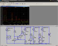
Okay, it's been several posts, but... CCS DISTORTION!
Yes, solid state CCS's have distortion because of their nonlinear output impedance (very nonlinear). I like the thought about avoiding phase/response anomalies in the output impedance, but output impedance itself is important because it determines how much distortion is injected by the CCS.
I suppose the question is, at what point does CCS distortion exceed capacitor distortion? Does it?
Here are THD plots of the CCS's, at 34V pk-pk, 10mA, commonly found in the VAS.
Also, would it not be okay to connect the shield to the output and leave it unconnected at the other end?
- keantoken
Attachments
Last edited:
Concerning the baxendall CCS , I got it to sim in isolation no problem. when I used it to source a VAS or LTP , it "fell apart". At under 3ma or with a large modulated load (vas) it was quite "squirrelly "Okay, it's been several posts, but... CCS DISTORTION!
Yes, solid state CCS's have distortion because of their nonlinear output impedance (very nonlinear). I like the thought about avoiding phase/response anomalies in the output impedance, but output impedance itself is important because it determines how much distortion is injected by the CCS.
I suppose the question is, at what point does CCS distortion exceed capacitor distortion? Does it?
Here are THD plots of the CCS's, at 34V pk-pk, 10mA, commonly found in the VAS.
Also, would it not be okay to connect the shield to the output and leave it unconnected at the other end?
- keantoken

Maybe if you could "plug it in" to an amp I could see it's benefits.
You should ground the shield , as this would negate any inductances from the OP bus or cap returns ...as you would have the wire under the board "sandwiched" between the FR-4 and the heatsink/chassis.
OS
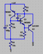
That is what I said , used as a "strait" CCS , as you post them .. they work - all of them. But , I try to plug them into an ampDid you use the "normal" version, or the tweaked one? The tweaked ones may give trouble... After all it is only an experiment. Try the one that I just posted in the schematic, exactly as shown.
- keantoken
they "poop the bed". BTW , I tried the tweaked one first then the normal one , both worked in isolation perfectly but I had great difficulty with the more complex application.here, plug it into the AX (2 CCS's), see if you can get it to work.. (below)
OS
Attachments
Last edited:
Try the one that I just posted in the schematic, exactly as shown.
- keantoken
IF that doesn't work, try this.
- keantoken
Attachments
I suppose the question is, at what point does CCS distortion exceed capacitor distortion? Does it?
- keantoken
The question is rather what is the real importance of a CCS
as a THD source..
THD for a classical CCS implemented with a bjt and a voltage
reference is in the order of a few ppm, while the distorsion
due to the VAS itself is about 1 % and soaring with high
voltages swings...
I really would like to use this CCS on my experimental board ,the FX , which already has a super pair. (below)
Try it , you will like..
I am not leaving these factors any room with those 2 cap multipliers on the pb250 , RIPPLE is the enemy !
OS
Try it , you will like..
By wahab - The question is rather what is the real importance of a CCS
as a THD source..
THD for a classical CCS implemented with a bjt and a voltage
reference is in the order of a few ppm, while the distorsion
due to the VAS itself is about 1 % and soaring with high
voltages swings...
I am not leaving these factors any room with those 2 cap multipliers on the pb250 , RIPPLE is the enemy !
OS
Attachments
Last edited:
Good point Wahab. Others say the CCS is audible and that is why I'm investigating. It's probably of little significance. However a weak CCS will disrupt LTP balance at HF and cause phase shifted LTP currents.
- keantoken
indeed it is audible if designed this way :
http://www.diyaudio.com/forums/soli...iews-comments-here-please-46.html#post2267574
indeed it is audible if designed this way :
http://www.diyaudio.com/forums/soli...iews-comments-here-please-46.html#post2267574
Ha , HA ...
"Designed" might be an improper term in this case. Carlos should of used 2 current sources like the AX.. 1/10th the distortion (I simmed his )OS
Good point Wahab. Others say the CCS is audible and that is why I'm investigating. It's probably of little significance. However a weak CCS will disrupt LTP balance at HF and cause phase shifted LTP currents.
- keantoken
I have noticed that the LTP balance actually gets better up and beyond 10Khz with the 2 tranny CCS's .. very noticable on the AX and CX.
OS
Ostripper, quiet you. That is a schematic from Doug Self's book! Carlos's amp uses a bootstrap, if you look at the beginning of that thread.
- keantoken
But he has the other one too , without the bootstrap. 100pF miller and all.
OS
Okay, I digress, the LTP of Carlos's amp uses a weak CCS.
For some reason the AC impedance of the voodoo CCS is the same as the two-Q version, in spite of the much lower DC impedance. This I do not understand.
Wait a sec - Ah! Ostripper, your KSC3503 model is botched I think... Try this one:
.MODEL SC3503 NPN IS=7.010E-13 BF=156.09 VAF=600 IKF=0.12325 ISE=1.2538E-14 NE=1.5 BR=0.64499 VAR=100 IKR=0.05102 ISC=6.4644E-09 NC=1.5 RE=0.108 RC=1.215 RB=12.134 RBM=0.034 IRB=3.0e-6 CJE=7.10E-12 CJC=8.20E-12 TF=7.025E-10 XTF=2 VTF=35 ITF=1 TR=1.0E-8 EG=0.76 XTB=1.5 FC=0.5
- keantoken
Okay, I digress, the LTP of Carlos's amp uses a weak CCS.
For some reason the AC impedance of the voodoo CCS is the same as the two-Q version, in spite of the much lower DC impedance. This I do not understand.
Wait a sec - Ah! Ostripper, your KSC3503 model is botched I think... Try this one:
.MODEL SC3503 NPN IS=7.010E-13 BF=156.09 VAF=600 IKF=0.12325 ISE=1.2538E-14 NE=1.5 BR=0.64499 VAR=100 IKR=0.05102 ISC=6.4644E-09 NC=1.5 RE=0.108 RC=1.215 RB=12.134 RBM=0.034 IRB=3.0e-6 CJE=7.10E-12 CJC=8.20E-12 TF=7.025E-10 XTF=2 VTF=35 ITF=1 TR=1.0E-8 EG=0.76 XTB=1.5 FC=0.5
- keantoken
"Botched"
it is the genuine fairchild model. I put yours in , no difference. Back to the topic of CCS's , it is alright to "share" the LED or diode referenced CCS's between LTP and VAS (my "supersym" has a RED LED CCS), but they are rather low performance to begin with. The 2 transistor ones work best alone since they are based on the gain of the transistors rather than an external referance.
OS
Last edited:
A question , Keen. Why do you use LT instead of multisim or microcap. And do you believe all models are created equal.
I have noticed that the newer models along with LT can simulate problems (oscillation , saturation) MUCH more reliably. I have multisim and it is too easy(optimistic). Where a circuit WILL work in multisim , sometimes it will not work or oscillate in LT. Could it be that LT's output is a more realistic representation of the real world ???
OS
- Status
- This old topic is closed. If you want to reopen this topic, contact a moderator using the "Report Post" button.
- Home
- Amplifiers
- Solid State
- The MONGREL (supersym II)